Exposure apparatus, exposure method, and device manufacturing method

Inactive Publication Date: 2005-07-05
NIKON CORP
View PDF34 Cites 56 Cited by
  • Summary
  • Abstract
  • Description
  • Claims
  • Application Information

AI Technical Summary

Benefits of technology

[0034]In addition, in a lithographic process, by performing exposure using the exposure apparatus in the present invention, the pattern can be formed with good accuracy on the substrate, allowing production of microdevices with higher integration with good yield. Similarly, in the lithographic process, by employing one of the first and the second exposure methods in the present inventio

Problems solved by technology

However, when it comes to measuring fine patterns of 0.13 μm and under, the measurement technique having the process of using equipment such as the above SEM has its limits.
This is because of reasons such as: errors may occur in reticle manufacturing such as fabricating errors of measurement patterns, errors may be caused in the process of resist coating and development of the substrate, or errors and deterioration of measurement reproducibility may occur when equipment such as the SEM is used.
In this method, however, when the environment changes in between a state where the projection optical system stands alone and a state where the projection optical system has been incorporated into the main body of the exposure apparatus, or when an accident occurs during the incorporation into the main body of the exposure apparatus, quality

Method used


Image

  • Exposure apparatus, exposure method, and device manufacturing method
  • Exposure apparatus, exposure method, and device manufacturing method
  • Exposure apparatus, exposure method, and device manufacturing method

Examples


Embodiment Construction

[0043]Referring to FIGS. 1 to 5, an embodiment of the present invention is described below.

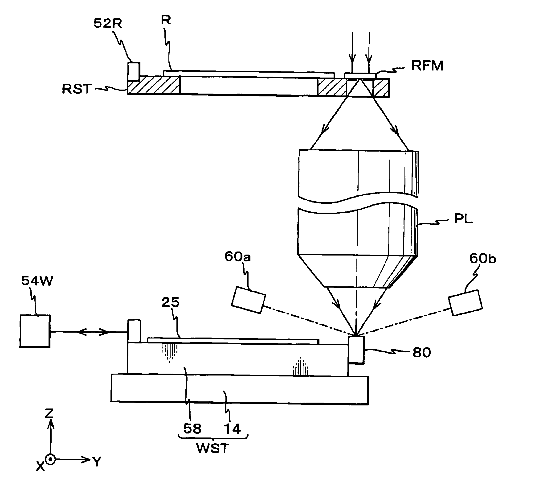
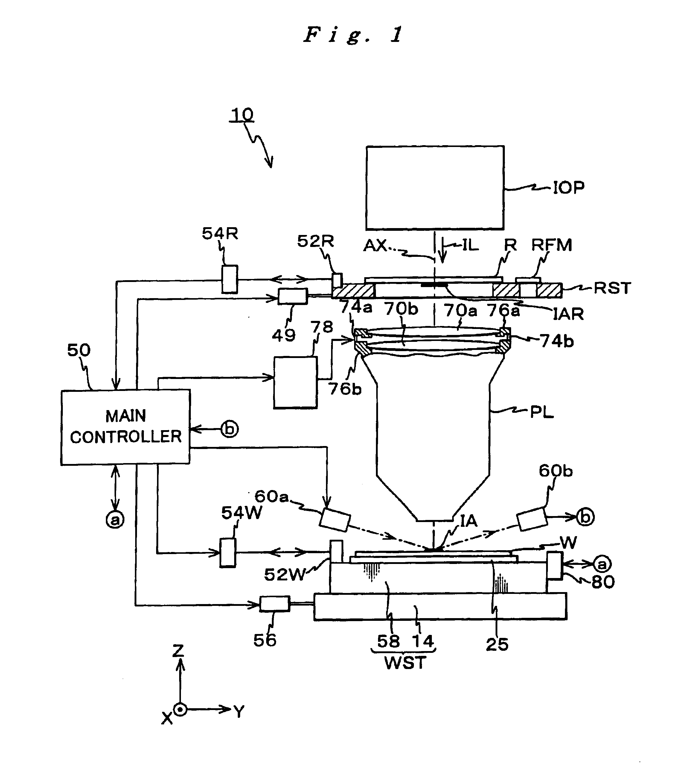
[0044]FIG. 1 shows an entire configuration of an exposure apparatus 10 related to the embodiment. Exposure apparatus 10 is a scanning exposure apparatus, based on a step-and-scan method.

[0045]Exposure apparatus 10 comprises: an illumination system IOP made up of a light source (not shown) and an illumination optical system; a reticle stage RST that holds a reticle R serving as a mask, which is illuminated with an illumination light for exposure (hereinafter simply referred to as “illumination light”) IL emitted from illumination system IOP; a projection optical system PL that projects illumination light IL outgoing from reticle R onto a wafer W serving as a substrate; a wafer stage WST that holds wafer W and serves as a substrate stage; a control system for these parts, and the like.

[0046]Illumination system IOP is structured including a light source, an illuminance uniformity optical system i...


PUM


Abstract

A fiducial plate on which at least one pinhole shaped pattern is formed is fixed on a mask stage, which moves holding a mask. Therefore, for example, wavefront aberration of a projection optical system can be measured without using any special kind of masks for measurement, by setting a wavefront measurement instrument of the attaching type to a substrate stage, illuminating the fiducial plate with an illumination system, and receiving spherical waves generated at the pinhole shaped pattern via projection optical system with the wavefront measurement instrument. Accordingly, the wavefront aberration of the projection optical system can be measured easily, at a desired timing, which allows sufficient quality control to be performed on the projection optical system. As a consequence, the pattern of the mask can be accurately onto the substrate, using the projection optical system on which sufficient quality control is performed.

Description

CROSS-REFERENCE TO RELATED APPLICATIONS[0001]This is a continuation of International Application PCT / JP02 / 00974, with an international filing date of Feb. 6, 2002, the entire content of which being hereby incorporated herein by reference, which was not published in English.BACKGROUND OF THE INVENTION[0002]1. Field of the Invention[0003]The present invention relates to exposure apparatus, exposure methods, and device manufacturing methods, and more particularly, to an exposure apparatus and an exposure method used in a lithographic process for manufacturing electronic devices such as a semiconductor device as in an LSI, a liquid crystal display device, a pick-up device as in a CCD, or a thin-film magnetic head, when transferring a pattern formed on a mask or a reticle (hereinafter generally referred to as a “reticle”) onto a substrate such as a wafer, and a device manufacturing method using the exposure apparatus and exposure method.[0004]2. Description of the Related Art[0005]Circui...

Claims


Application Information

Patent Timeline
IPC IPC(8): G03F7/20
CPCG03F7/70591G03F7/706H01L21/027
Inventor ISHIKAWA, JUN
Owner NIKON CORP
Why Eureka
Try Eureka