Semiconductor device and method of manufacturing semiconductor device

Active Publication Date: 2006-12-14
SONY CORP
View PDF6 Cites 55 Cited by
  • Summary
  • Abstract
  • Description
  • Claims
  • Application Information

AI Technical Summary

Benefits of technology

[0029] In this method of manufacturing a semiconductor device, the first gate electrode material layer is covered by the second gate electrode material layer in the first trench in which the gate of the first conduction type MOS transistor is formed; therefore, when polishing is so conducted as to leave the electrode metal layer in the first trench and the second trench, the layers exposed to the surface are the electrode metal layer, the second gate electrode material layer and the gate insulation film. Therefore, since the number of layers exposed is reduced, as compared with the number of kinds of metallic layers exposed at the time of polishing in the related art, so that galvanic corrosion is generated with difficulty. In addition, since the electrode metal layer can be formed inside the first trench and the second trench by polishing the electrode metal layer and the second gate electrode material layer, polishing wi

Problems solved by technology

For polishing (CMP) of four kinds of materials constituting the electrode metallic material layer, the metal gate material for the nMOS transistor, the metal gate material layer for the pMOS transistor and the gate insulation film, it may be necessary to regulate the selection ratios among the total of five kinds of materials including the four kinds of materials to be polished and an under film (e.g., silicon oxide (SiO2)), and it is highly difficult to develop abrasives (slurries).
In addition, since a plurality of films are polished, it is difficult to stabilize the scatterings of processing, due to the presence o

Method used


Image

  • Semiconductor device and method of manufacturing semiconductor device
  • Semiconductor device and method of manufacturing semiconductor device
  • Semiconductor device and method of manufacturing semiconductor device

Examples


Example

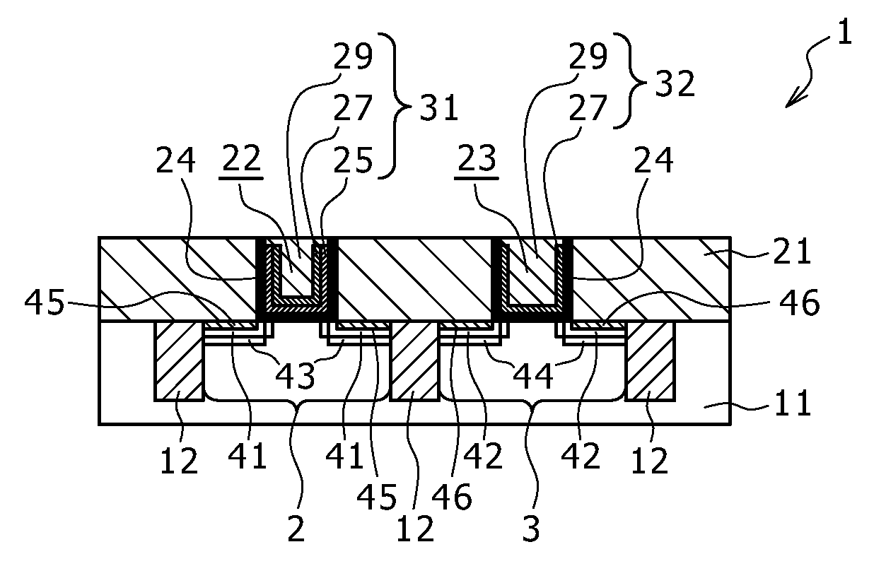
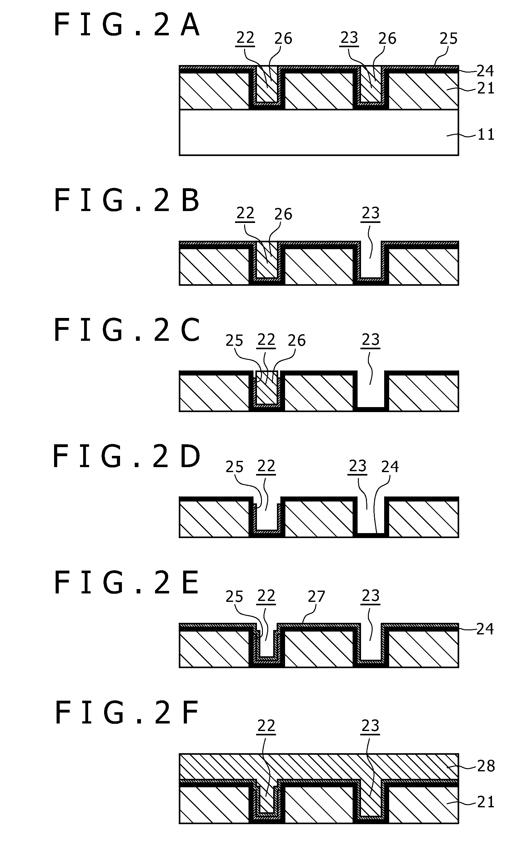
[0038] Now, a first example of an embodiment of the semiconductor device in the present invention will be described below, referring to a schematic configuration sectional diagram shown in FIG. 1.

[0039] As shown in FIG. 1, a first conduction type (p-type) MOS transistor 2 and a second conduction type (n-type) MOS transistor 3 of the type opposite to the first conduction type are formed in a substrate 11 in the state of being isolated by a device isolation region 12, to constitute a semiconductor device 1. An insulation film 21 formed on the substrate 11 is provided with a first trench 22, and a gate electrode 31 of the p-type MOS transistor 2 is formed in the first trench 22. In addition, the insulation film 21 is provided with a second trench 23, and a gate electrode 32 of the n-type MOS transistor 3 is formed in the second trench 23.

[0040] A first gate electrode material layer 25 of the first conduction type MOS transistor, a second gate electrode material layer 27 of the second...


PUM


Abstract

A semiconductor device including, on a substrate, a first conduction type MOS transistor having a gate electrode provided in a first trench formed in an insulation film on the substrate, and a second conduction type MOS transistor having a gate electrode provided in a second trench formed in the insulation film, the first conduction type and the second conduction type being opposite types.

Description

CROSS REFERENCES TO RELATED APPLICATIONS [0001] The present invention contains subject matter related to Japanese Patent Application JP 2005-172031 filed in the Japanese Patent Office on Jun. 13, 2005, the entire contents of which being incorporated herein by reference. BACKGROUND OF THE INVENTION [0002] 1. Field of the Invention [0003] The present invention relates to a semiconductor device and a method of manufacturing the same by which it is possible to prevent galvanic corrosion from occurring in a dual metal gate structure. [0004] 2. Description of the Related Art [0005] Transistors with a higher degree of integration and a higher operating speed have been realized by miniaturization of the transistors, based on the scaling rule. Thinning of the gate insulation film has progressed, and in a transistor of a gate length of, for example, 0.1 μm or less, it may be necessary to reduce the thickness of the gate insulation film to or below 2 nm. [0006] As a gate electrode material, no...

Claims


Application Information

Patent Timeline
IPC IPC(8): H01L29/78H01L21/8238
CPCH01L21/28079H01L21/823842H01L29/42368H01L29/6659H01L29/495H01L29/4958H01L29/66545H01L29/42376
Inventor NAGAHAMA, YOSHIHIKO
Owner SONY CORP
Why Eureka
Try Eureka