

Airgap-containing interconnect structure with patternable low-k material and method of fabricating
Inactive Publication Date: 2009-07-09
GLOBALFOUNDRIES INC
View PDF11 Cites 115 Cited by
- Summary
- Abstract
- Description
- Claims
- Application Information
AI Technical Summary
Benefits of technology
[0067]This patternable low-k / inorganic ARC method of present invention dramatically reduces the complexity in the fabrication of current interconnect structures. The photoresist used in the prior art integration is no longer needed. In addition to not requiring a separate photoresist, the present invention also does not utilize a plasma etching step for patterning as also required in the prior art interconnect processing schemes. It is further noted that the inventive method reduces the number of layers required to fabricate the interconnect structure and, as such, the present invention reduces the time and cost of fabricating interconnect structures as compared to prior art processes.
Problems solved by technology
Unfortunately, conventional organic antireflective coatings are generally not suitable for the lithography of a patternable low-k material as the antireflective coating layer is a permanent part of the interconnect structure.
These organic antireflective coatings typically cannot withstand high temperature processes such as, for example, the high temperature during either the curing of the patternable low-k dielectric or annealing of the interconnect metal.
Method used
View moreImage
Smart ImageViewing Examples

Examples
second embodiment
[0098]In a second embodiment, a Si:C:O:H film is deposited under the following conditions: precursor=tetramethylsilane at a flow of 10 sccm mixed with oxygen at a flow of 2 sccm, pressure in reactor=200 mtorr, substrate temperature=180° C., substrate bias=−200 V.
third embodiment
[0099]In a third embodiment, a Si:C:H film is deposited under the following conditions: precursor=trimethylsilane at a flow of 10 sccm, pressure in reactor=200 mtorr, substrate temperature=60° C., substrate bias=−200 V.
fourth embodiment
[0100]In a fourth embodiment, a Si:C:O:H film is deposited under the following conditions: precursor=trimethylsilane at a flow of 10 sccm mixed with oxygen at a flow of 2 sccm, pressure in reactor=200 mtorr, substrate temperature=60° C., substrate bias=−200 V.
Login to View More PUM
 Abstract
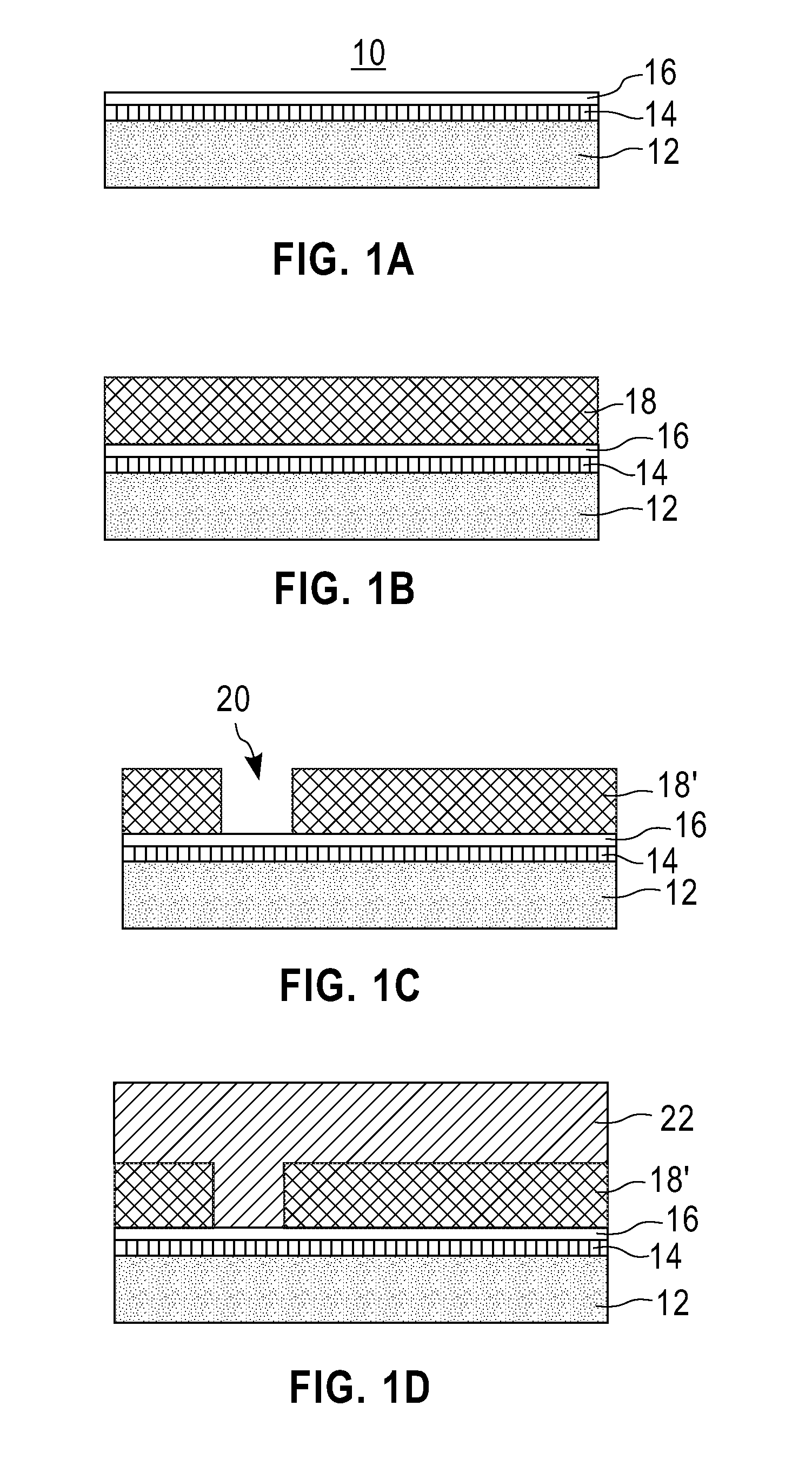
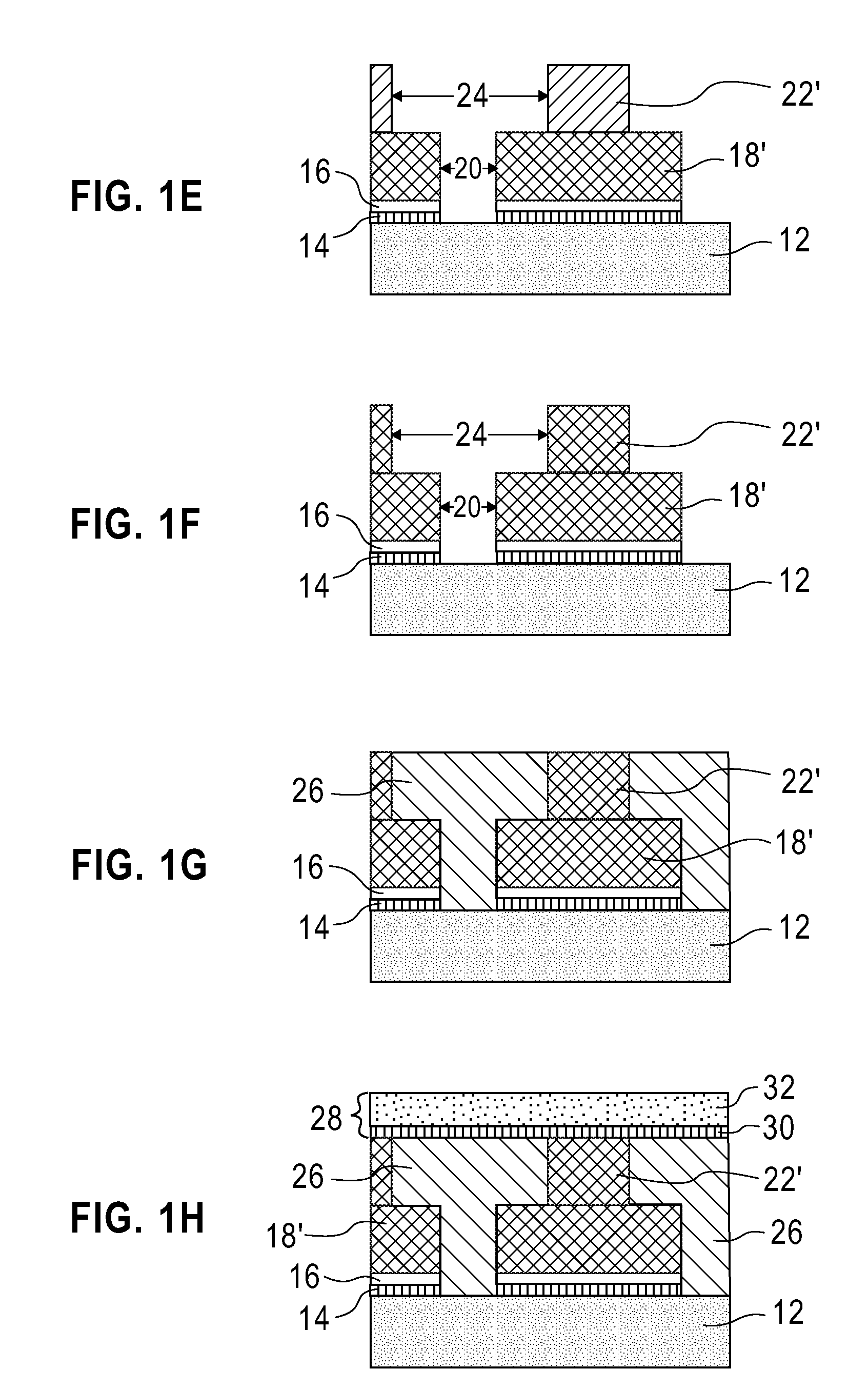
The present invention provides a method of fabricating an airgap-containing interconnect structure in which a patternable low-k material replaces the need for utilizing a separate photoresist and a dielectric material. Specifically, this invention relates to a simplified method of fabricating single-damascene and dual-damascene airgap-containing low-k interconnect structures with at least one patternable low-k dielectric and at least one inorganic antireflective coating.
Description
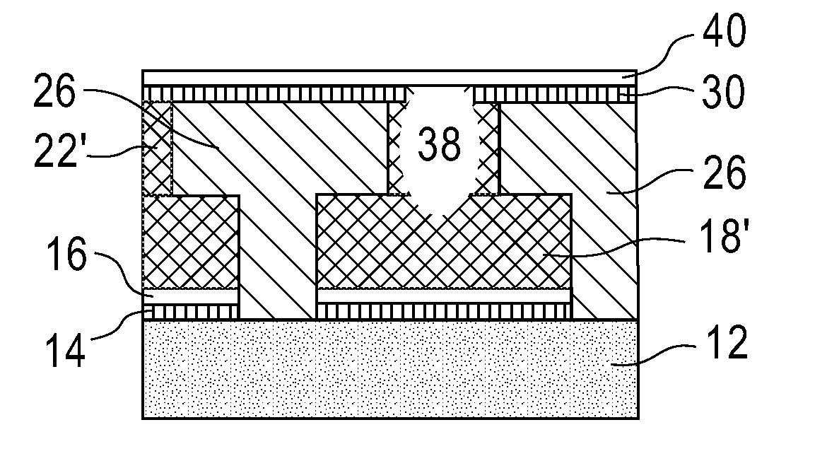
FIELD OF THE INVENTION [0001]The present invention relates to an interconnect structure and a method of fabricating the same. More specifically, the present invention relates to an interconnect structure including a patternable dielectric material as an interconnect dielectric and at least one airgap within the patternable dielectric material. The present invention also provides a method of fabricating such a patternable dielectric interconnect structure.BACKGROUND OF THE INVENTION [0002]It is widely known that the speed of propagation of interconnect signals is one of the most important factors controlling overall circuit speed as feature sizes are reduced and the number of devices per unit area as well as the number of interconnect levels are increased. Throughout the semiconductor industry, there has been a strong drive to increase the aspect ratio (i.e., height to width ratio) and to reduce the dielectric constant, k, of the interlayer dielectric (IDS) materials used to electric...
Claims
Login to View More Application Information
Patent Timeline
 IPC IPC(8): H01L21/768H01L23/538
CPCH01L21/76808H01L21/7682H01L21/76835H01L23/5222H01L23/5329H01L23/53295H01L2924/0002H01L2924/12044H01L23/532H01L2924/00
InventorLIN, QINGHUANG
OwnerGLOBALFOUNDRIES INC