Stud, circuit board device using the stud, and method of mounting the circuit board device

Inactive Publication Date: 2010-05-27
NEC COMPUTERTECHNO LTD
View PDF3 Cites 2 Cited by
  • Summary
  • Abstract
  • Description
  • Claims
  • Application Information

AI Technical Summary

Benefits of technology

[0013]According to the present invention, the stud is surface-mounted on the printed circuit board, so that it is possible to eliminate the need to form a hole for the stud in the printed circuit board. This allows the wiring density of the printed circuit board to be reduced to thereby reduce noise due to h

Problems solved by technology

This makes signals on the pattern wiring more likely to be affected by noise to deteriorate signal quality.
When the number of layers of the printed circuit board is increased so as not to allow the pattern wiring density to increase, cost of the printed circuit board becomes higher.
This ma

Method used


Image

  • Stud, circuit board device using the stud, and method of mounting the circuit board device
  • Stud, circuit board device using the stud, and method of mounting the circuit board device
  • Stud, circuit board device using the stud, and method of mounting the circuit board device

Examples


Example

FIRST EXAMPLE

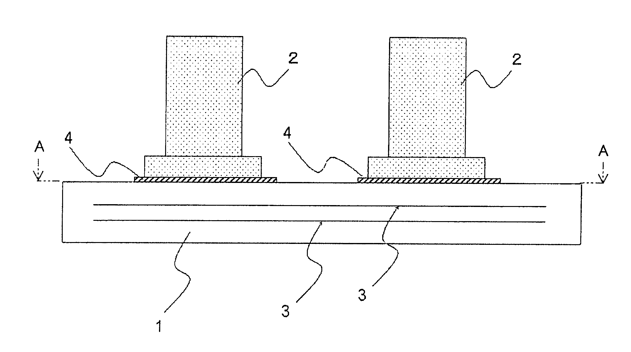
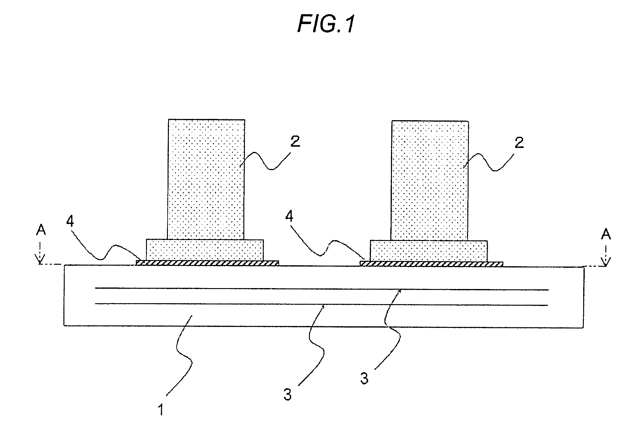
[0030]A first example of the present invention will be described with reference to FIG. 3.

[0031]A circuit board device according to the present example shown in FIG. 3 includes a plate 13, a printed circuit board 12 having a pattern wiring (not shown) which is disposed on the plate 13, and a plurality of surface mount type studs 14 which are columnar-shaped structures for mezzanine mounting, on the printed circuit board 12, a small printed circuit board (another printed circuit board) 15 which is a mounting component having a smaller dimension than the printed circuit board 12 by fixing thereto by means of a screw (locking screw) 16.

[0032]The surface mount type stud 14 of the present example has a columnar-shaped main body. One end of the main body in the axial direction is secured to a component pad 17 provided on the printed circuit board 12 by soldering as in the case of other surface mount type electronic components (not shown), whereby the surface mount type stud ...

Example

SECOND EXAMPLE

[0034]A second example of the present invention will be described below with reference to FIG. 4.

[0035]Although the basic structure of a circuit board device according to the present example is the same as that of the circuit board device according to the first example, a further twist has been added to the structure of the surface mount type stud. The configuration is shown in FIG. 4.

[0036]A circuit board device shown in FIG. 4 includes a plate 13, a printed circuit board 12 having a pattern wiring (not shown) which is disposed on the plate 13, and a plurality of surface mount type studs 14a which are columnar-shaped structures for mezzanine mounting, on the printed circuit board 12, a small printed circuit board 15 which is a mounting component having a smaller dimension than the printed circuit board 12 by fixing thereto by means of a screw 16.

[0037]The surface mount type stud 14a according to the present example is a separate type stud constituted by a plurality o...

Example

THIRD EXAMPLE

[0045]A third example of the present invention will be described with reference to FIG. 5.

[0046]In a circuit board device according to the third example, a further twist has been added to the structure of the surface mount type stud according to the second example. The configuration is shown in FIG. 5.

[0047]A circuit board device shown in FIG. 5 includes a plate 13, a printed circuit board 12 having a pattern wiring (not shown) which is disposed on the plate 13, and a plurality of surface mount type studs 14b which are columnar-shaped structures for mezzanine mounting, on the printed circuit board 12, a small printed circuit board 15 which is a mounting component having a smaller dimension than the printed circuit board 12 by fixing thereto by means of a screw 16.

[0048]As in the case of the second example, the surface mount type stud 14b according to the present example is a separate type stud constituted by a plurality of structural parts that can adjust the relative p...


PUM

PropertyMeasurementUnit
Structureaaaaaaaaaa

Abstract

A stud is a structure for supporting, on a printed circuit board, a mounting component such as another printed circuit board or a device. This structure is surface-mounted on the printed circuit board by soldering or press-fitting. The structure is a constituted by a columnar-shaped structure and the like. One end of the columnar-shaped structure is surface-mounted on the printed circuit board, and the other end thereof is fixed to the mounting component.

Description

[0001]This application is based upon and claims the benefit of priority from prior Japanese Patent Application No. 2008-300848, filed Nov. 26, 2008, the entire contents of which are incorporated herein.TECHNICAL FIELD[0002]The present invention relates to a stud, a circuit board device using the stud, and a method of mounting the circuit board device and, more particularly, to a stud structure for supporting a mounting component on a printed circuit board.BACKGROUND ART[0003]In general, in order to achieve miniaturization of a computer apparatus, there is required, e.g., an increase in the integration degree of devices. As one of approaches for increasing the integration degree, there is known a method in which a printed circuit board is formed in a mezzanine structure to be made three-dimensional. In this method, a stud which is a structure for fixing, on a printed circuit board, a mounting component, such as another printed circuit board or a device, is used.[0004]FIG. 6 shows a c...

Claims


Application Information

Patent Timeline
IPC IPC(8): H05K1/14H05K1/00H05K3/00
CPCH05K1/18H05K1/181H05K3/308Y10T29/49124H05K2201/10318H05K2201/10409H05K2201/105H05K3/341Y02P70/50
Inventor YOKOUCHI, KAZUHITO
Owner NEC COMPUTERTECHNO LTD
Why Eureka
Try Eureka