Touch panel with improved linear response and minimal border width electrode pattern

a technology of linear response and electrode pattern, applied in the field of touch screen panels, can solve the problems of reducing the usable touch screen space, the size of the electrode pattern, and the cost of linearization efforts, and achieve the effect of improving linear response and minimal border width edge electrode pattern

Inactive Publication Date: 2003-07-24
3M INNOVATIVE PROPERTIES CO
View PDF1 Cites 28 Cited by
  • Summary
  • Abstract
  • Description
  • Claims
  • Application Information

AI Technical Summary

Benefits of technology

[0009] It is therefore an object of this invention to provide a touch panel with an improved linear response and minimum border width edge electrode pattern.
[0010] It is a further object of this invention to provide such a touch panel at a low cost and using manufacturing techniques which result in a higher yield.
[0011] It is a further object of this invention to provide such a touch screen panel which is simple to manufacture and uses simpler electrode configurations.
[0012] This invention results from the realization that the linearity of a touch screen panel can be improved at the same time the size and especially the width of the electrode pattern is reduced not by complex electrode configurations but instead by a continuous repeating pattern of rows of spaced electrode conductive segments wherein every row including the outermost row has at least two conductive segments facing three conductive segments in the next adjacent inner row. In this way, the number of gaps is increased but each gap can be made smaller and the rows placed closer together resulting in improved linearity and a smaller size electrode pattern both of which increases the usable touch screen space.
[0013] A touch screen panel comprising an insulative substrate, a resistive layer on the insulative substrate, and a plurality of spaced conductive segments on the resistive layer along the border thereof, the conductive segments disposed in rows, every row having at least two segments each facing at least a portion of three segments in an adjacent row for improving the linearity of the touch screen panel and at the same time reducing the space occupied by the conductive segments on the touch screen panel.

Problems solved by technology

In general, however, linearization efforts come at a cost: namely, the size of the electrode pattern, because linearization can be optimized by increasing the number of rows of electrode segments, or the complexity by producing the insulated segments in the electrode pattern.
These efforts, in turn, increase the size, and in particular the width of the electrode pattern along the border of the touch screen panel thereby reducing the usable touch screen space, or increase the manufacturing complexity and cost.
The second factor is the complexity in manufacturing these electrode patterns, which indicates the cost factor.
These electrodes can occupy considerable space along the edge of the touch sensor.
Therefore, a larger electrode pattern will partially invade the display's viewable area, rendering the touch sensor unusable.
None of the prior art electrode pattern configurations satisfactorily resolve all three factors and must sacrifice either linearity, narrow width or simplicity.
The MicroTouch electrode pattern occupies a considerable amount of space.

Method used


Image

  • Touch panel with improved linear response and minimal border width electrode pattern
  • Touch panel with improved linear response and minimal border width electrode pattern
  • Touch panel with improved linear response and minimal border width electrode pattern

Examples


Embodiment Construction

[0019] Other objects, features and advantages will occur to those skilled in the art from the following description of a preferred embodiment and the accompanying drawings, in which:

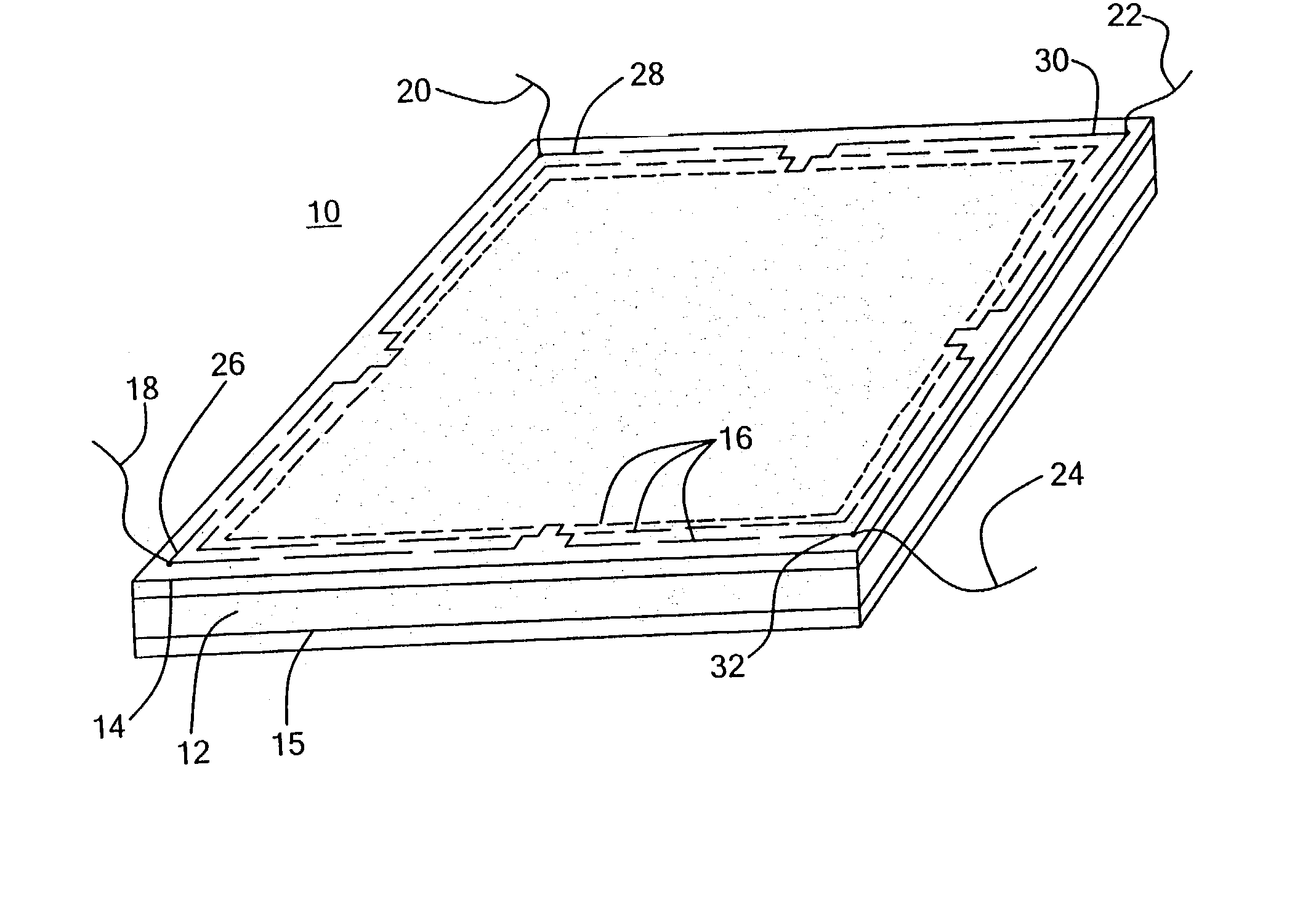
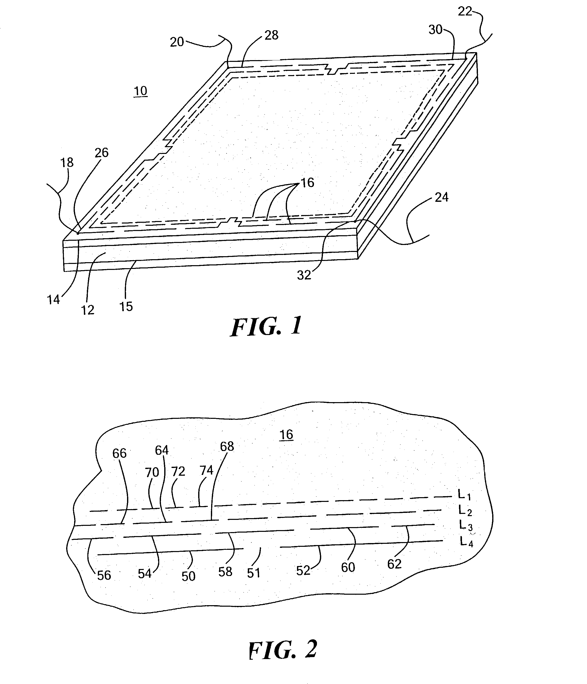
[0020] FIG. 1 is a schematic three-dimensional view of the touch screen panel in accordance with the subject invention;

[0021] FIG. 2 is a schematic view of the unique electrode conductive segment pattern for the border areas of the touch screen panel shown in FIG. 1;

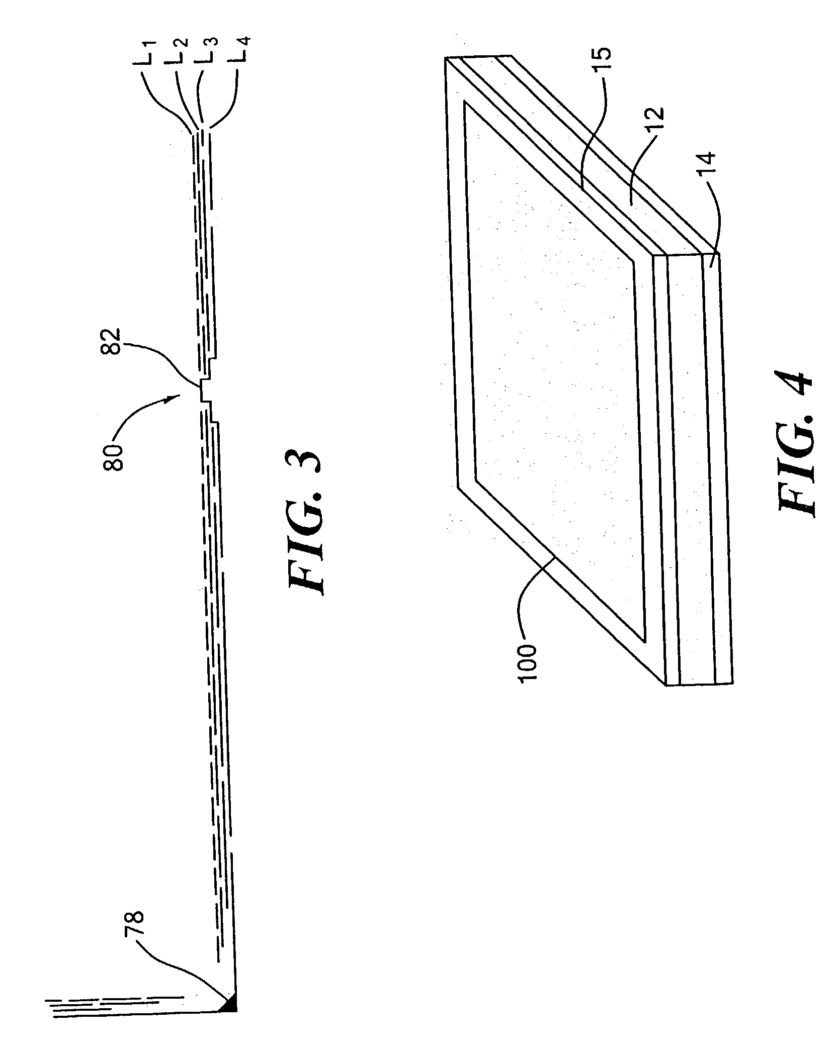
[0022] FIG. 3 is top view of a portion of the electrode pattern on the border area of the touch screen shown in FIG. 1;

[0023] FIG. 4 is a schematic three-dimensional view of the bottom of the touch screen panel shown in FIG. 1;

[0024] FIG. 5 is cross-sectional view of an embodiment of a resistive touch screen panel in accordance with the subject invention;

[0025] FIG. 6 is a schematic top view of one embodiment of the subject invention wherein conductive leads are deposited on a dielectric layer disposed over the resistive layer of the touch sc...


PUM


Abstract

A touch screen panel including an insulative substrate; a resistive layer disposed on the insulative substrate; and a plurality of spaced conductive segments on the resistive layer along the border thereof. The conductive segments are disposed in rows, and every row has at least two segments which face at least a portion of three segments in the next inner row for optimizing the linearity of the touch screen panel and at the same time reducing the space occupied on the touch screen panel by the conductive segments.

Description

[0001] This invention relates to touch screen sensors and in particular to the electrode pattern formed on the border of the resistive layer of the touch screen panel.BACKGROUND OF INVENTION[0002] Touch screen panels generally comprise an insulative (e.g. glass) substrate and resistive layer disposed on the insulative substrate. A pattern of conductive electrodes are then formed on the edges of the resistive layer. The conductive electrodes form orthogonal electric fields in the X and Y direction across the resistive layer. Contact of a finger or stylus on the panel then causes the generation of a signal that is representative of the x and y coordinates of the location of the finger or stylus with respect to the substrate. In this way, the associated touch panel circuitry can ascertain where the touch occurred on the substrate.[0003] Typically, a computer program generates an option to the user (e.g. "press here for `yes` and press here for `no`") on a monitor underneath the touch s...

Claims


Application Information

Patent Timeline
Patent Type & Authority Applications(United States)
IPC IPC(8): G06F3/033G06F3/044G06F3/045
CPCG06F3/044G06F2203/04113G06F3/045G06F3/0443
Inventor HUANG, JIANMINGGEAGHAN, BERNARD O.
Owner 3M INNOVATIVE PROPERTIES CO
Why Eureka
Try Eureka