

X-ray fluorescence spectrometer for semiconductors
a fluorescence spectrometer and semiconductor technology, applied in semiconductor/solid-state device testing/measurement, material analysis using wave/particle radiation, instruments, etc., can solve the problem that the damaged circuit patterned area of the semiconductor wafer or the whole wafer cannot be used for circuit chips for shipment, and the per-piece cost of the semiconductor wafer increases
- Summary
- Abstract
- Description
- Claims
- Application Information
AI Technical Summary
Problems solved by technology
Method used
Image

Examples
first embodiment
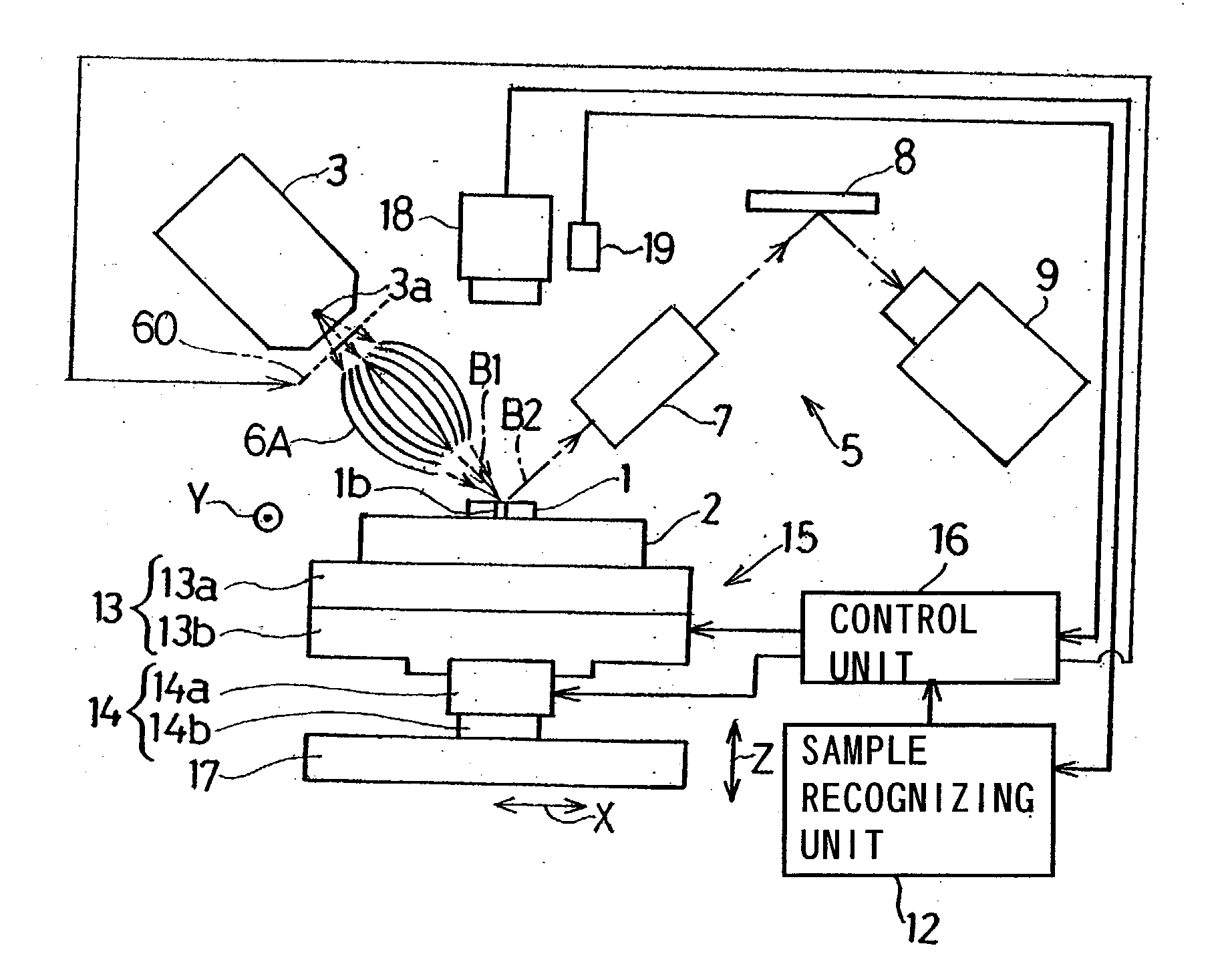
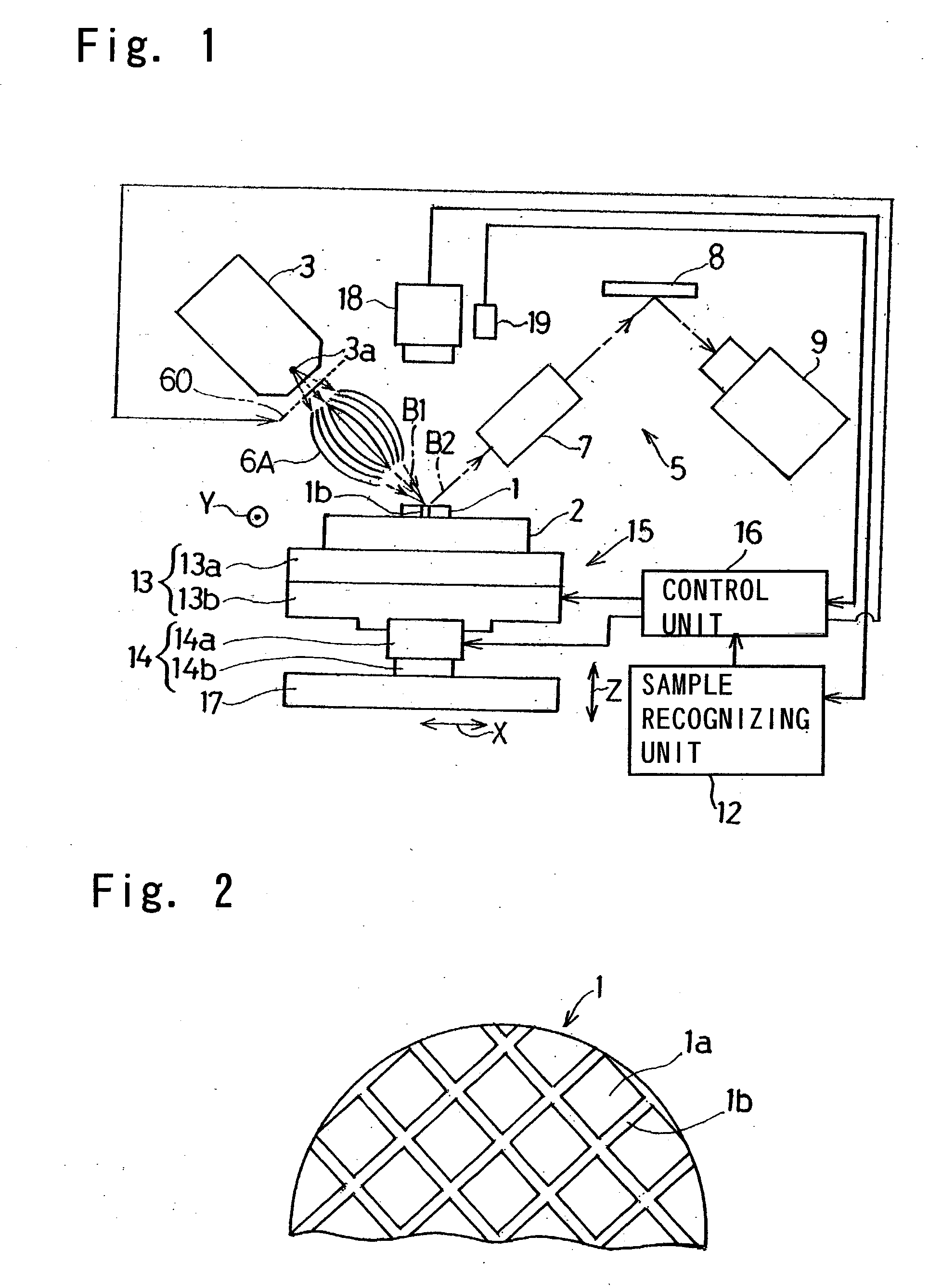
[0040] As discussed above, with the X-ray fluorescence spectrometer according to the present invention, the scribe line 1b of the semiconductor wafer 1 is recognized as the target site of measurement and the scribe line 1b of the semiconductor wafer 1 is so positioned by the positioning mechanism 15 that only the scribe line 1b of the semiconductor wafer 1 can be irradiated with the primary X-rays B1 which have been converged by the poly-capillary 6A to a spot size not greater than 50 .mu.m. With the scribe line 1b of the semiconductor wafer 1 so measured in the manner described above, the semiconductor wafer 1 can be analyzed non-invasively without the circuit patterned areas 1a being detrimentally damaged by irradiation with the primary X-rays B1, and at an inexpensive cost with no need to use a dedicated semiconductor sample hitherto required solely for the purpose of measurement.
[0041] In the foregoing description, the two-dimensional focusing element has been described as emplo...
second embodiment
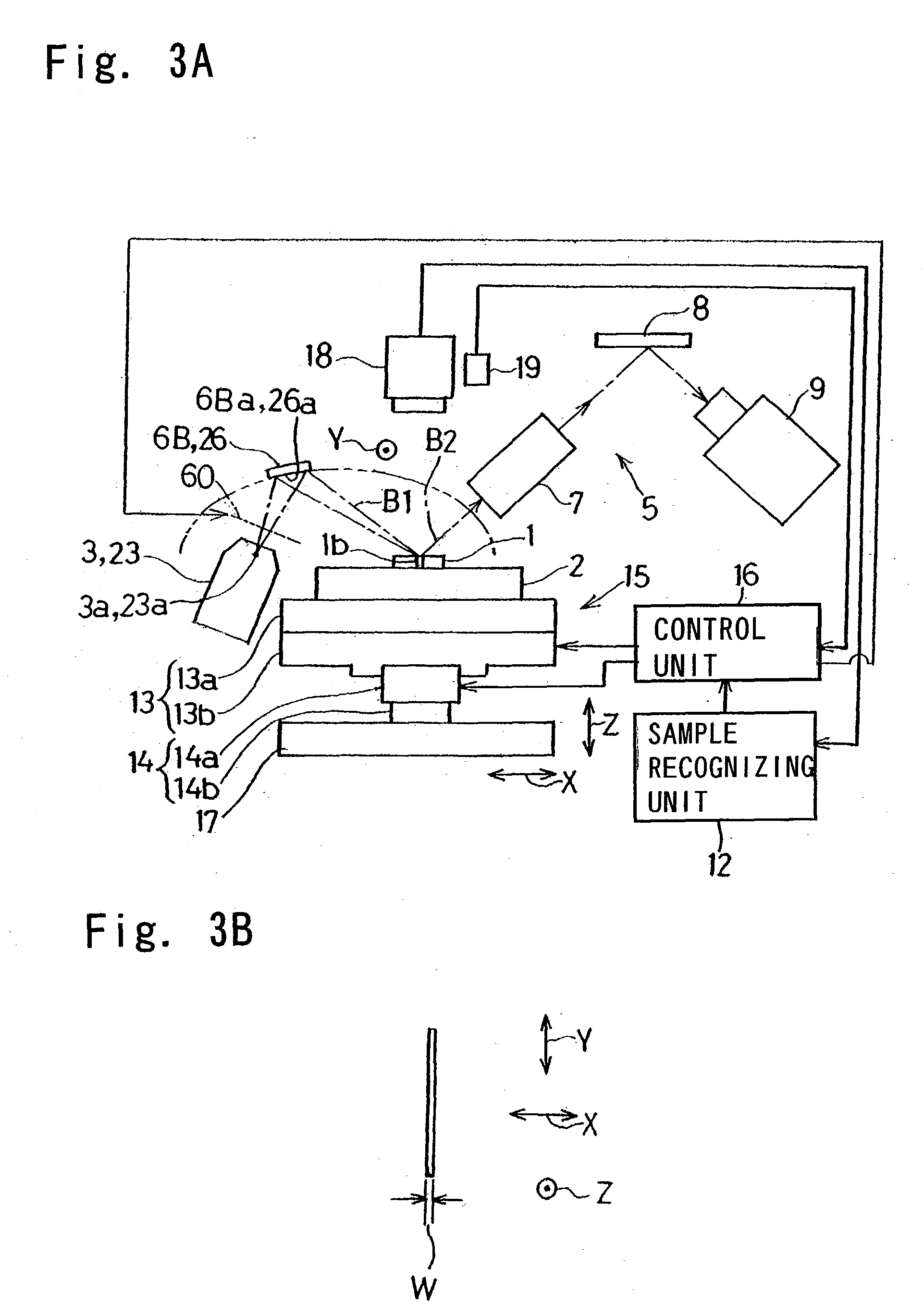
[0045] The one-dimensional focusing element 26 that can be employed in the X-ray fluorescence spectrometer may be a mirror or spectroscopic device 26 having a reflecting surface 26a of an elliptic cylindrical shape or a cylindrical shape approximating to the elliptic cylindrical shape. Where the one-dimensional focusing element 26 is employed in the form of the mirror and the X-rays from the source of primary X-rays 23a undergoes a total reflection when impinging upon the reflecting surface 26a because of a small angle of incidence thereof on the reflecting surface 26a, the shape of the reflecting surface 26 may be a sphere approximating to the elliptic cylinder. By way of example, the one-dimensional focusing element 26 in the form of the mirror having the elliptic cylindrical reflecting surface 26a is of such a design in which the reflecting surface 26a occupies a portion of an elliptic cylinder that extends in a direction perpendicular to the plane of the sheet of the drawing, a...
third embodiment
[0048] The crisscross focusing element 36 employed in the practice of the present invention may be of a design including, as shown in FIG. 7A, two pairs of opposed mirrors or spectroscopic devices 36-1 and 36-2, 36-3 and 36-4 arranged with a direction of confrontation of the opposed mirrors or spectroscopic devices 36-1 and 36-2 lying perpendicular to a direction of confrontation of the opposed mirrors or spectroscopic devices 36-3 and 36-4. In such case, each of the mirrors or spectroscopic devices 36-1 to 36-4 of the focusing element 36 has a respective reflecting surface 36-1a, 36-2a, 36-3a and 36-4a that is an elliptic cylindrical shape or a cylindrical shape approximating to the elliptic cylindrical shape. Where the focusing element 36 is employed in the form of the mirrors and the X-rays from the source of primary X-rays 3a undergoes a total reflection when impinging upon the corresponding reflecting surface 36a because of a small angle of incidence thereof on the reflecting s...
PUM
| Property | Measurement | Unit |
|---|---|---|
| diameter | aaaaa | aaaaa |
| width | aaaaa | aaaaa |
| size | aaaaa | aaaaa |
Abstract
Description
Claims
Application Information