Semiconductor wafer support lift-pin assembly

a technology of semiconductor wafers and lift pins, which is applied in the direction of chucks, mechanical apparatus, manufacturing tools, etc., can solve the problems of lift pins loosing, increasing size, and affecting so as to reduce the space required below the support platform, raise and lower a semiconductor wafer, and increase the conductance of gasses

Inactive Publication Date: 2003-11-06
APPLIED MATERIALS INC
View PDF3 Cites 225 Cited by
  • Summary
  • Abstract
  • Description
  • Claims
  • Application Information

AI Technical Summary

Benefits of technology

[0011] A plurality of lift-pin holes extends through the support platform, the base, the substrate support, and circumscribe the centrally disposed recess. Each of the modular lift-pin assemblies respectively extends (i.e., slidably extends) through the plurality of lift-pin holes, and a C-shaped lift-arm assembly disposed below the base engages the plurality of lift-pin assemblies to raise and lower a semiconductor wafer. The lift-arm assembly passes into a slot in the support platform, thus reducing the space required below the support platform to operate the lift-pins. The reduced space requirement allows for the support platform to be positioned closer to a pumping stack and thereby increasing the conductance of gasses through the chamber.

Problems solved by technology

Integrated circuits have evolved into complex devices that include millions of transistors, capacitors and resistors on a single chip.
One problem that has been observed is that the lift-pins may bind as they pass through the lift-pin holes in the substrate support.
Another problem is that the increased size in the industry from 200 mm to 300 mm wafers requires redesign of the processing chambers and accordingly, the lift-pin assemblies with regard to their configuration with other components in the substrate support assembly.

Method used


Image

  • Semiconductor wafer support lift-pin assembly
  • Semiconductor wafer support lift-pin assembly
  • Semiconductor wafer support lift-pin assembly

Examples


first embodiment

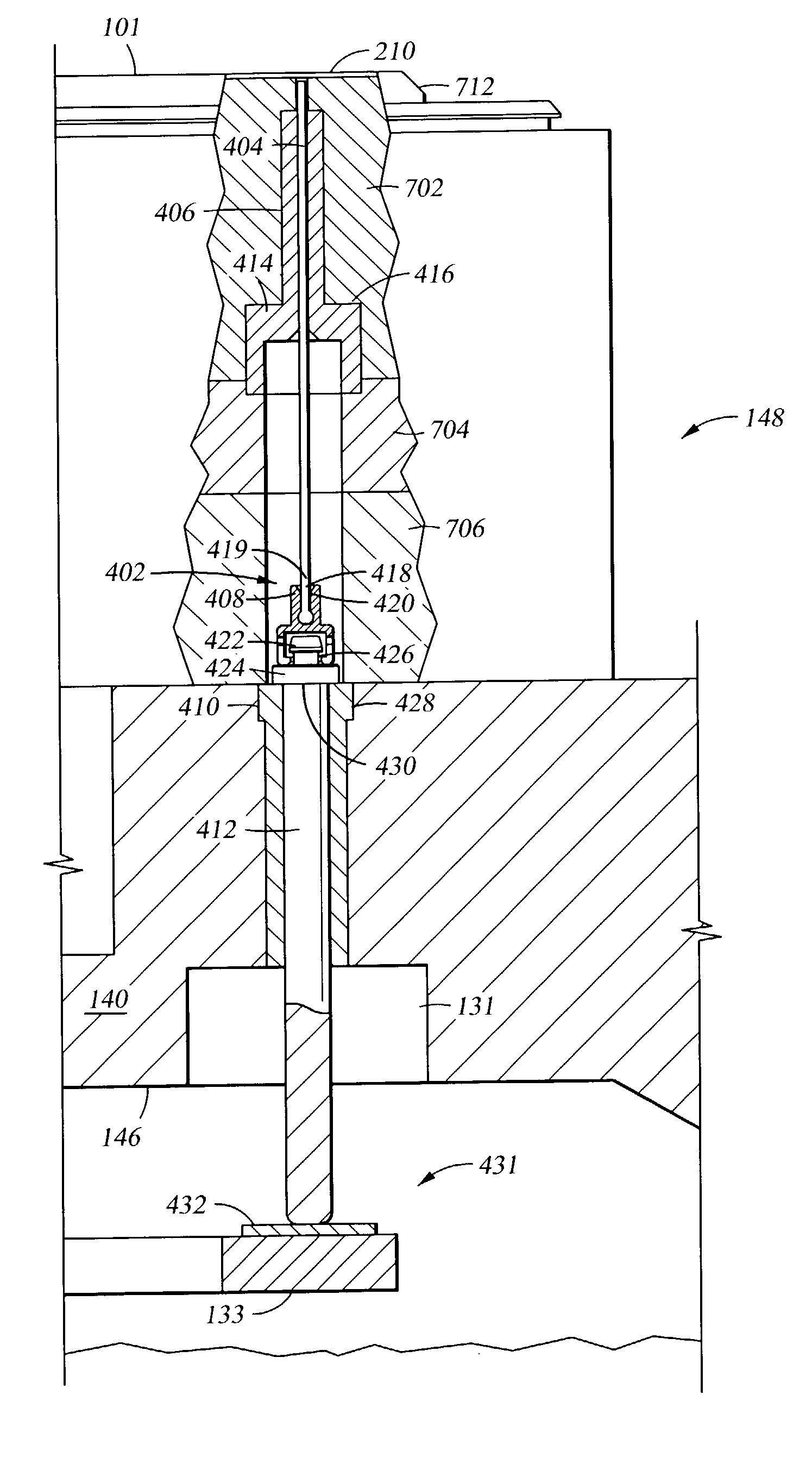
[0042] FIGS. 5A and 5B are perspective views of the connector 408 of the lift-pin assembly 402 of FIG. 4. The connector 408 comprises a first end (i.e., actuator end) 501 and a second end (i.e., lift-pin end) 509, where the first end 501 has a diameter that is greater than a diameter of the second end 509. The connector 408 is typically a polymer suitable for use in a support assembly 148 such as VESPEL.RTM.. The first and second ends 501 and 509 of the connector 408 each comprise a plurality of catch fingers 502a and 502b (collectively, catch fingers 502). In one embodiment, four exemplary catch fingers 502 are illustratively disposed on each end 501 and 509 of the connector 408, however it will be appreciated that the catch fingers may vary in quantity. Each finger 502a and 502b includes a lip 504a and 504b that extends radially inwards. Each lip 504a and 504b includes a flat 506a and 506b that is substantially perpendicular to a central axis 512 extending a length of the connecto...

second embodiment

[0045] FIGS. 9A and 9B depict perspective views of a connector 908 of the lift-pin assembly of FIG. 4. The connector 908 shown in FIGS. 9A and 9B is the same as the connector 408 depicted in FIGS. 5A and 5B, except that only the fingers 502a on the first end 501 include a lip 504a that extends radially inwards. Further, each lip 504a includes a flat 506a that is substantially perpendicular to a central axis 512 extending a length of the connector 908. It is further noted that the second end 509 of the connector 908 comprises a bore 420 that is sized to allow the distal end 418 of the lift-pin 404 to be inserted into the bore 420 of the second end 509 of the connector in a secure manner.

[0046] It is noted that four exemplary catch fingers 502 are illustratively disposed on each end 501 and 509 of the connector 908, however it will be appreciated that the number of catch fingers may vary in quantity. Furthermore, in an alternate embodiment, the second end 509 may comprise only a cylin...


PUM

PropertyMeasurementUnit
diametersaaaaaaaaaa
sizeaaaaaaaaaa
diameteraaaaaaaaaa

Abstract

A modular lift-pin assembly includes a lift-pin having a distal end, a connector, and an actuator pin. The connector includes an actuator end having a plurality of catch fingers disposed around the actuator end. Each of the plurality of catch fingers includes a lip extending radially inwards. A lift-pin end is coupled to the distal end of the lift-pin, and the actuator pin is coupled to the actuator end of the connector.

Description

CROSS REFERENCE[0001] This application is a Continuation-in-Part of U.S. patent application Ser. No. 09 / 797,214, filed Feb. 28, 2001, which claims benefit of U.S. Provisional Application No. 60 / 185,283, filed Feb. 28, 2000, which are hereby incorporated by reference in their entireties.BACKGROUND OF THE DISCLOSURE[0002] 1. Field of Invention[0003] The present invention relates generally to an apparatus for processing semiconductor wafers. More specifically, the invention relates to a lift-pin assembly for moving semiconductor wafer using in a semiconductor wafer-processing chamber.[0004] 2. Description of the Background Art[0005] Integrated circuits have evolved into complex devices that include millions of transistors, capacitors and resistors on a single chip. The evolution of chip design results in faster circuitry and greater circuit density. As the demand for integrated circuits continues to rise, chip manufactures have demanded semiconductor process tooling having increased wa...

Claims


Application Information

Patent Timeline
Patent Type & Authority Applications(United States)
IPC IPC(8): C23C16/40C23C16/44C23C16/458
CPCC23C16/405C23C16/4401C23C16/4409Y10T279/11C23C16/45561C23C16/4586Y10T279/23C23C16/4412
Inventor GUJER, RUDOLFCHO, THOMAS K.PANG, LILY L.KARAZIM, MICHAEL P.ISHIKAWA, TETSUYA
Owner APPLIED MATERIALS INC
Why Eureka
Try Eureka