Method and apparatus for three-dimensional integration of embedded power module

a power module and three-dimensional integration technology, applied in the direction of process and machine control, magnetic bodies, instruments, etc., can solve the problems of increasing heat dissipation, inability to implement in the integrated circuit with the actives, and increasing clock speed, so as to reduce packaging overhead, improve electrical efficiency, and reduce packaging overhead

Inactive Publication Date: 2011-04-26
VIRGINIA TECH INTPROP INC
View PDF6 Cites 16 Cited by
  • Summary
  • Abstract
  • Description
  • Claims
  • Application Information

AI Technical Summary

Benefits of technology

[0018]It is another object of the invention to provide a three-dimensional integrated module, having a high conductance embedded LTCC inductor with high current capability, in a low profile layered arrangement, with short interlayer electrical connections, providing a low-profile and high-efficiency.
[0019]It is another object of the invention to provide a three-dimensional integrated module, having a high conductance embedded LTCC inductor, and having a planar, low profile shape and aspect ratio, for smaller size and for significantly improved air flow over the apparatus.
[0029]According to its various embodiments, a three-dimensional integrated module of the present invention reduces packaging overhead as compared to the prior art. The packaging overhead is reduced in part because the high conductance LTCC inductor functions both in an electrical capacity and a structural capacity; its large area planar top and bottom surfaces function as support surfaces for circuitry and for heat sink structures.
[0030]According to its various embodiments, the three-dimensional integrated module of the present invention improves electrical efficiency over the prior art. The layered structure allows short interlayer connections, without jumps and with minimum lateral traces.
[0031]One or more embodiments of the present invention include a planar heat spreader with the invention's high-conductance planar LTCC inductor. These and other embodiments of the invention, in addition to providing reduced packaging overhead, include a high thermal conduction, large area, distributed heat carrying structure—effectively the entire area of any layer or layers the module. This provides even spreading of heat from concentrated heat sources over a large planar area. This provides significant thermal improvement over prior art structures. Further, the planar, low profile module of the embodiments and their various aspects provides less turbulent airflow.

Problems solved by technology

However, typically, one or more of the reactive elements has a large value (i.e., microfarads or microhenrys) and, therefore, cannot be practically implemented in the integrated circuit with the actives.
Heat dissipation is an increasing problem with SVRs, because their power requirements are increasing.
Increasing computational power requires more complex semiconductor circuits, i.e., more transistors and interconnects, and higher clock speed that, in turn, increases power consumption.
The SVR heat dissipation problem is often exacerbated because, in addition to delivering more power, the SVR must be physically smaller packages.
For example, resistive loss wastes battery power, lowers the power actually delivered by the SVR, and increases the heat the SVR generates.
Since the structure of the SVR must accommodate this heat, but the heat represents wasted power, the SVR design or the powered circuit design may have to be compromised, to meet overall power and heat budget.
The concurrent demand for SVR higher power and smaller SVR packages, presents problems that are difficult to solve with present SVR circuit technologies.
Because of high current and low resistance requirements, these SVR inductors are generally implemented as separate components, packaged and arranged in a manner occupying area on a substrate and often requiring long connection paths.
However, known LTCC inductors are generally unsuitable for high current applications such as, for example, power supplies or voltage regulators.
They are unsuitable because the inductive elements are thin, high resistance conductors that cannot carry high current.
Because of the printed conductor structure of LTCC inductors, the conductive wiring formed from the conductive ink is too thin to carry large currents.
These and other limitations and shortcomings have prevented LTCC inductors from being used in high power electronics applications and, instead, has relegated LTCC inductors to applications such as RF filters, tuners and the like.
Prior art high power SVRs are therefore constructed with discrete inductors and associated connections, with resulting resistive losses and stray reactance.
Further, the discrete inductors and other structural features of prior art SVRs often result in heat sources, requiring heat conduction and heat sink structures that occupy volume.
Further, the discrete inductors and other structural features of prior art SVRs often require that the heat sources be arranged for practical thermal connection with heat sinks, and these arrangements may compromise the electrical performance of the SVR.

Method used


Image

  • Method and apparatus for three-dimensional integration of embedded power module
  • Method and apparatus for three-dimensional integration of embedded power module
  • Method and apparatus for three-dimensional integration of embedded power module

Examples


Embodiment Construction

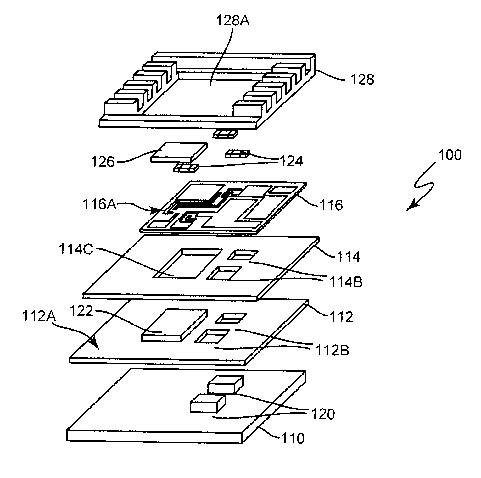
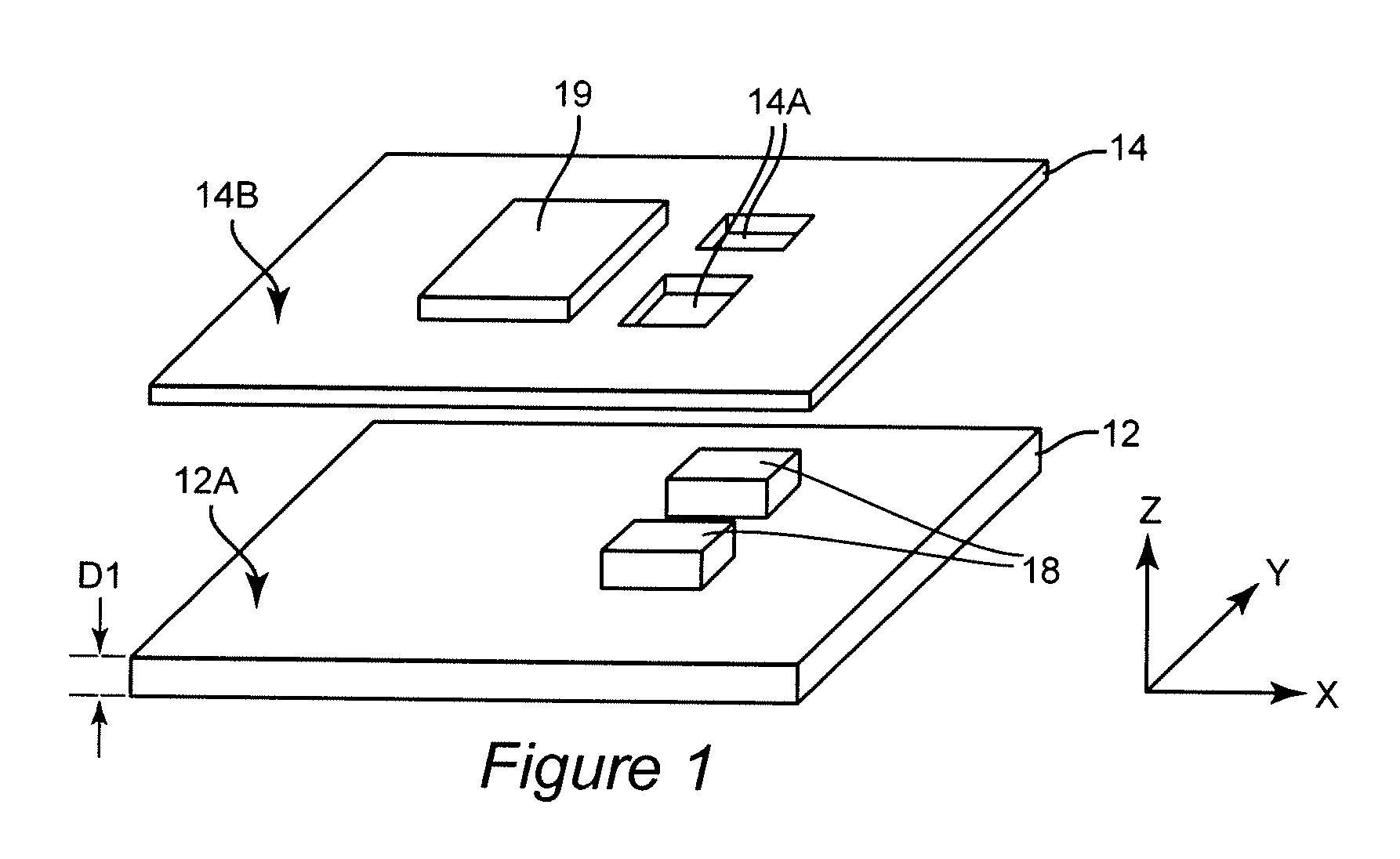
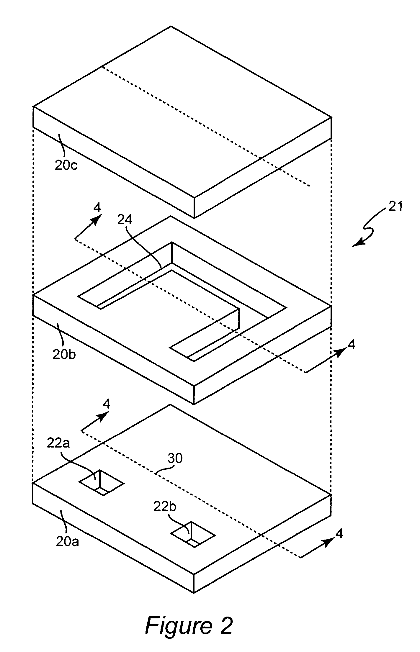
[0051]The following detailed description of the invention is in reference to accompanying drawings, which form a part of this description but are only illustrative examples of various embodiments in which the invention may be practiced. The invention is not limited, however, to the specific examples described herein and / or depicted by the attached drawings. Other configurations and arrangements embodying or practicing the present invention can, upon reading this description, be readily implemented by persons skilled in the arts.

[0052]In the drawings, like numerals appearing in different drawings, either of the same or different embodiments of the invention, reference functional or system blocks that are, or may be, identical or substantially identical between the different drawings.

[0053]Various embodiments of the invention, although different, are not necessarily mutually exclusive. For example, a particular feature, function, act or characteristic described in one embodiment may, ...


PUM

PropertyMeasurementUnit
thickaaaaaaaaaa
thickaaaaaaaaaa
thickaaaaaaaaaa

Abstract

A modified planar Low Temperature Co-Fired Ceramic (LTCC) high conductance inductor, embedding a large cross section conductor, supports a stacked arrangement of heat spreader, inductor and active device layers. Interlayer electrical connections connect the layers. Optionally, a DC-DC converter includes the modified planar LTCC high conductance inductor, embedding a large cross section conductor, supporting a stacked arrangement of heat spreader, capacitor and active device layers, the active devices layer including the switching transistors. The active devices layer may include semiconductor dies embedded in a substrate.

Description

CROSS-REFERENCE TO RELATED APPLICATION(S)[0001]This patent application is a continuation-in-part (CIP) of U.S. patent application Ser. No. 11 / 357,424, filed Feb. 21, 2006 now U.S. Pat. No. 7,638,988, the specification of which is incorporated herein by reference.[0002]This invention was made with United States Government support under Grant No. EEC9731677, awarded by the National Science Foundation. The United States Government may have certain rights in this invention.FIELD OF THE INVENTION[0003]The present invention relates generally to circuit and component technology and, more specifically, to switching-type power regulation circuits having requirements for high power and small packaging.BACKGROUND OF THE INVENTION[0004]As known in the art, a switching voltage regulator (SVR) receives an electrical power from a source such as, for example, a battery or AC-DC rectifier, and outputs electrical power at a controlled or regulated voltage.[0005]A typical SVR includes transistor-based...

Claims


Application Information

Patent Timeline
Patent Type & Authority Patents(United States)
IPC IPC(8): H01F27/08H02M3/335H01F7/06H01F27/28H01F29/06H01H63/00
CPCH01F17/0033H02M3/155H01F41/043H01F38/42Y10T29/4902H01F2017/002H02M3/158H01F5/00
Inventor LIM, MICHELE H.LIANG, ZHENXIANVAN WYK, J. D.
Owner VIRGINIA TECH INTPROP INC
Why Eureka
Try Eureka