Optical waveguide platform and method of manufacturing the same

a technology of optical waveguides and platform, applied in the field of planar optical waveguide type optical modules, can solve the problems of difficult to precisely polish the lower clad layer, inability to easily integrate active devices such as laser diodes (ld) or photo diodes (pd), and inability to manufacture terrace patterns accurately

Inactive Publication Date: 2004-02-12
ELECTRONICS & TELECOMM RES INST
View PDF8 Cites 21 Cited by
  • Summary
  • Abstract
  • Description
  • Claims
  • Application Information

AI Technical Summary

Problems solved by technology

In manufacturing optical device on silicon substrate using a flame hydrolysis deposition and PE-CVD (plasma enhanced chemical vapor deposition), optical passive device such as optical waveguide can be fabricated, but active device such as a laser diode (LD) or a photo diode (PD) can not be integrated with ease.
Because of the unevenness generated in the lower clad layer due to the step of the terrace, the polishing process is required to planarize the lower clad layer.
Furthermore, a terrace pattern can not be manufactured accurately if crystallized direction of the silicon wafer is wrong.
Also, in polishing the lower clad layer of the optical waveguide, since the silica film of the lower clad layer has a thickness of several tens .mu.m, it is difficult to polish the lower clad layer precisely.
And, if the deviation in the poli

Method used


Image

  • Optical waveguide platform and method of manufacturing the same
  • Optical waveguide platform and method of manufacturing the same
  • Optical waveguide platform and method of manufacturing the same

Examples


Embodiment Construction

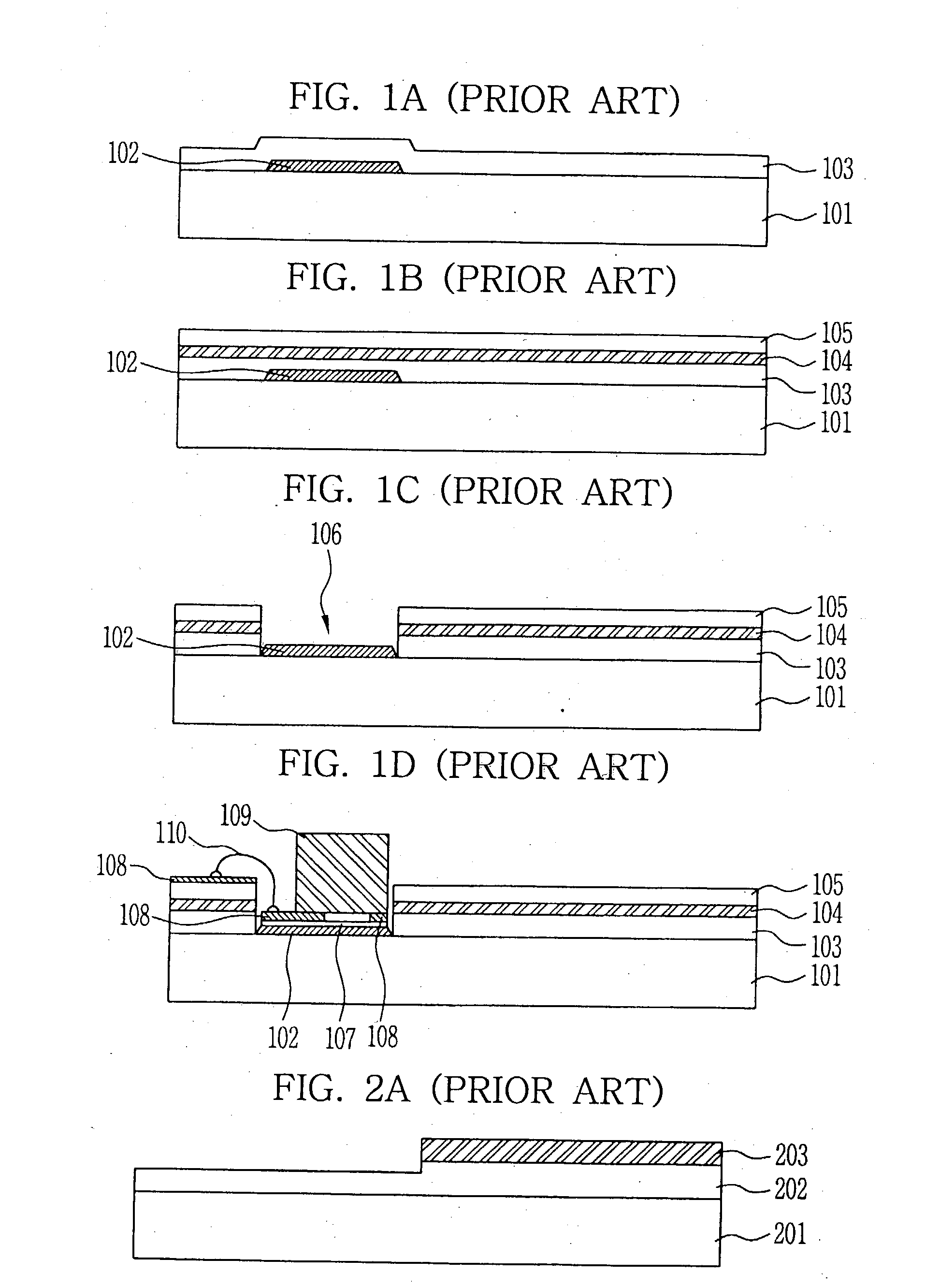
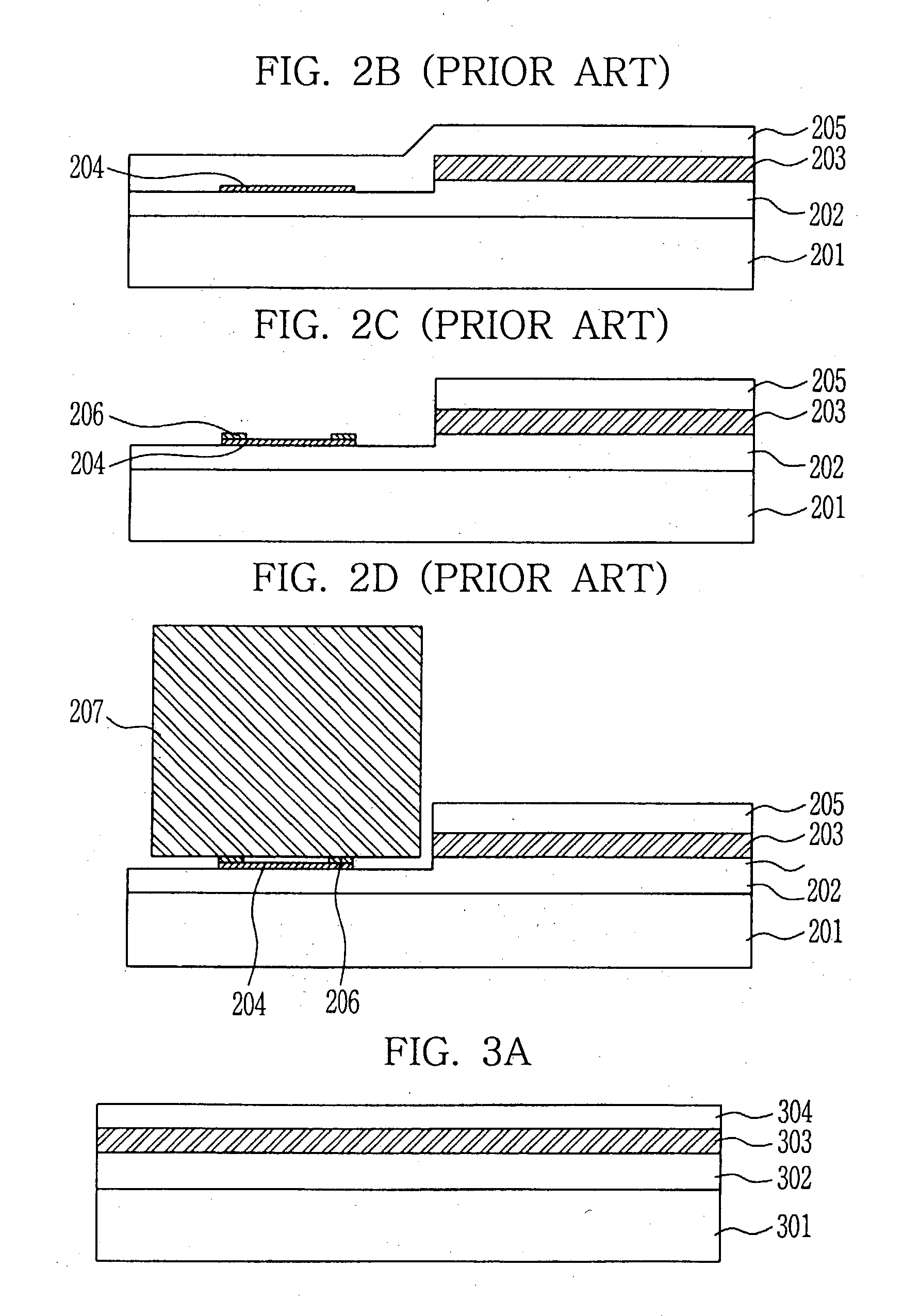
[0034] Hereinafter, the embodiments of the present invention will be explained with reference to the accompanying drawings. However, the embodiment of the present invention can be changed into a various type, and it should not be understood that the scope of the present invention is limit to the following embodiments. The embodiments of the present invention are provided in order to explain the present invention to those skilled in the art. Also, in drawings, a same reference numeral indicates a same element.

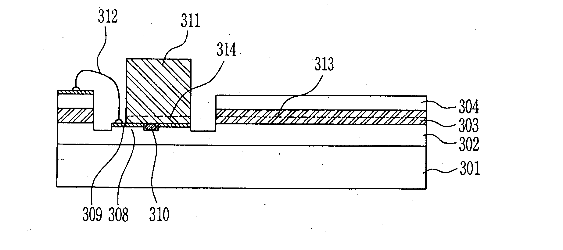
[0035] FIGS. 3A to 3E are cross-sectional views illustrating a method of manufacturing an optical waveguide platform according to the present invention in the process sequence.

[0036] Referring to FIG. 3A, a lower clad layer 302 is formed and a core layer 303 is stacked on a substrate 301 sequentially. The core layer 303 forms an optical waveguide core by patterning and etching processes. And, an upper clad layer 304 is formed on the core layer 303. The optical waveguide consists...


PUM


Abstract

An optical waveguide platform and a method of manufacturing the same are disclosed. The optical waveguide platform comprises an optical waveguide having a lower clad layer, a patterned core layer and an upper clad layer which are laminated on one area of said substrate sequentially, a terrace formed by patterning said lower clad layer, on the other area of said substrate, a metal and a solder formed on said terrace and an optical device mounted on said terrace containing said metal and said solder. According to the present invention, the optical waveguide platform can be manufactured in a simple method without damaging the optical waveguide and the manufacturing cost thereof can be reduced.

Description

[0001] 1. Field of the Invention[0002] The present invention relates to a planar optical waveguide type optical module and a method of manufacturing the same, more particularly, to an optical waveguide platform capable of mounting an optical device by a flip-chip bonding and a method of manufacturing the same.[0003] 2. Description of the Prior Art[0004] Recent technologies require the development of highly functional opto-electronic components. Opto-electronic hybrid integration using a silica planar lightwave circuit (PLC) is one promising method to satisfy the requirement. The combination of the PLC and active device leads to ahighly functional opto-electronic module for signal processing.[0005] In manufacturing optical device on silicon substrate using a flame hydrolysis deposition and PE-CVD (plasma enhanced chemical vapor deposition), optical passive device such as optical waveguide can be fabricated, but active device such as a laser diode (LD) or a photo diode (PD) can not be...

Claims


Application Information

Patent Timeline
IPC IPC(8): G02B6/12G02B6/42G02B6/13
CPCG02B6/12004G02B2006/12176G02B2006/12173G02B6/42G02B6/13
Inventor PARK, SANG HOSHIN, JANG UKPARK, YOON JUNGKIM, DUK JUNHAN, YOUNG TAKSUNG, HEE KEYNG
Owner ELECTRONICS & TELECOMM RES INST
Why Eureka
Try Eureka