Intermediate layer material composition for multilayer resist process and pattern formation process using the same
Inactive Publication Date: 2004-03-18
FUJIFILM HLDG CORP +1
View PDF0 Cites 10 Cited by
- Summary
- Abstract
- Description
- Claims
- Application Information
AI Technical Summary
Benefits of technology
0096] The alkoxymethyl group bonded to the benzene ring is preferably an alkoxymethyl group having 6 or less carbon atoms. Specifically, preferred are a methoxymethyl group, an ethoxymethyl group, a n-propoxymethyl group, an i-propoxymethyl group, a n-butoxymethyl group, an i-butoxymethyl group, a sec-butoxymethyl group and a t-butoxymethyl group. Further, an alkoxy-substituted alkoxyl group such as a 2-methoxyethoxy group or a 2-methoxy-1-propyl group is also preferred.
0097] Further, the molecular weight thereof is preferably from 250 to 1,000, and particularly preferably from 250 to 800.
0098] Of these phenol derivatives, particularly preferred ones are enumerated below: 23242526
0099] wherein L.sup.1 to L.sup.8, which may be the same or different, each represents a hydroxymethyl group, a methoxymethyl group or an ethoxymethyl group.
0100] The hydroxymethyl group-containing phenol derivatives can be obtained by reacting phenol compounds having no correspondi
Problems solved by technology
On the other hand, a lowering of the dimensional accuracy of resist patterns caused by fluctuations in resist film thickness based on differences in level of substrates which are developed in the fabrication of the semiconductor integrated circuits has occurred as a problem.
Aside from this, a more serious problem has been encountered.
Based on the shortened wavelengths of the exposure light sources, the light absorption of resist materials becomes increasingly strong, so that it becomes impossible to use conventional aromatic ring-based organic polymeric materials.
The situation has come in which conventional monolayer resist processes can no longer ensure sufficient dry etching resistance, thus making it impossible to process substrates with a high degree of accuracy.
However, these intermediate layer materials are essentially poor in storage stability.
Accordingly, they have the critical problem that line edge roughness (LER) is deteriorated when the intermediate layers are etched using the upper layer resist patterns as masks.
On the other hand, exceeding 70% by weight results in unfavorable stability of the intermediate layer material composition.
The presence of these impurities in large amounts unfavorably results in poor operation, defects and decreased yields in fabricating semiconductor devices.
The lower resist layer having a thickness of thinner than 0.1 .mu.m is unfavorable from the viewpoints of antireflection and etching resistance.
On the other
Method used
View moreImage
Smart ImageViewing Examples
Examples
 PUM
| Property | Measurement | Unit |
|---|---|---|
| Angle | aaaaa | aaaaa |
| Fraction | aaaaa | aaaaa |
| Fraction | aaaaa | aaaaa |
Abstract
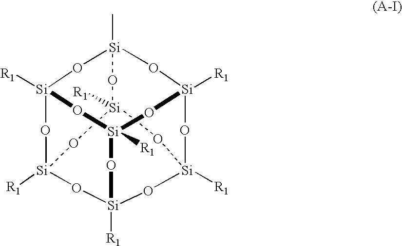
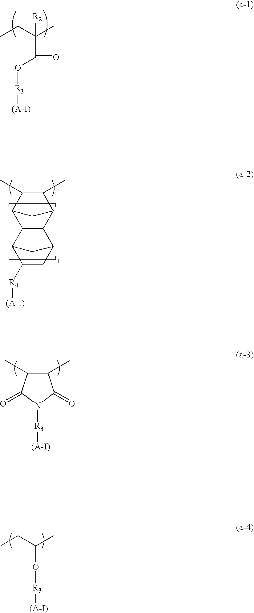
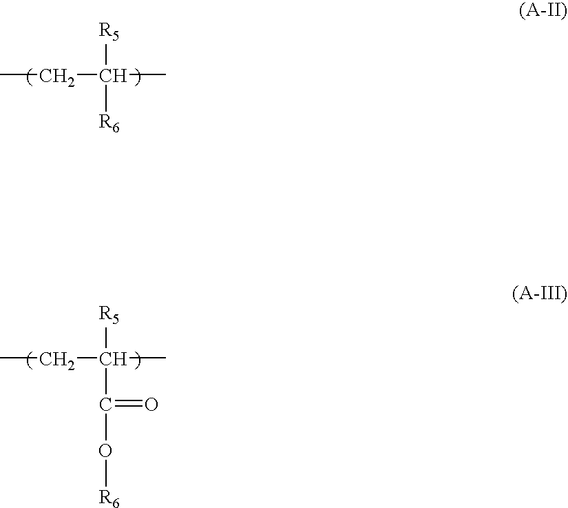
The intermediate layer material composition for a multilayer resist process in the present invention, which is soluble in an organic solvent, excellent in storage stability, and has no problem with regard to a footing shape, a pattern separation and a line edge roughness in patterning an upper resist, and a pattern formation process using the intermediate layer material composition, in which the intermediate layer material composition for a multilayer resist process, comprises a polymer (component A) containing a repeating unit having on a side chain thereof a specific structure containing a silicon atom-oxygen atom bond, and the pattern formation process using the same.
Description
[0001] The present invention relates to lithography technology by which a micro pattern is formed with a high degree of accuracy on a substrate in the fabrication of a semiconductor integrated circuit, and to an intermediate layer material composition for a multilayer resist process, particularly for a three-layer resist process and a pattern formation process using the same.BACKGRAOUND OF THE INVENTION[0002] With the progress of increased integration of semiconductor integrated circuits, resist patterns have been increasingly required to be miniaturized and raised in accuracy in lithography processes. In order to comply with this requirement, also in exposure methods, it has been intended to surely go ahead with the development of techniques for shortening the wavelengths of light sources toward the enhancement of resolution from the conventional near-ultraviolet lights such as g-rays and i-rays to excimer laser beams such as KrF, ArF and F.sub.2, EUV lights and X-rays.[0003] On th...
Claims
Login to View More Application Information
Patent Timeline
 IPC IPC(8): G03F7/075G03F7/09G03F7/11G03F7/26H01L21/027
CPCG03F7/0752G03F7/094Y10S430/114Y10S430/106G03F7/11
Inventor UENISHI, KAZUYASATO, KENICHIRO
Owner FUJIFILM HLDG CORP


