Method for forming introgen-containing oxide thin film using plasma enhanced atomic layer deposition

a technology of atomic layer deposition and introgen-containing oxide, which is applied in the direction of coating, chemical vapor deposition coating, coating process, etc., can solve the problems of low breakdown voltage, high leakage current, and low breakdown voltag

Inactive Publication Date: 2004-04-22
ELECTRONICS & TELECOMM RES INST
View PDF0 Cites 452 Cited by
  • Summary
  • Abstract
  • Description
  • Claims
  • Application Information

AI Technical Summary

Benefits of technology

[0011] Since the thin film formation method according to the present invention is based on ALD, the advantages of ALD, such as the ability to grow a dense, uniform thin film, are ensured. In addition, the use of plasma in the present invention further increases the density of the thin film and the growth rate. Furthermore, since a trace of nitrogen atoms can be incorporated in situ into the thin film being grown, the resulting thin film is provided with improved breakdown characteristics. The added nitrogen atoms improve the passivation properties for the incorporation of moist or impurities as well as the electrical properties.
[0012] In an embodiment of the present invention, a nitrogen-containing Al.sub.2O.sub.3 thin film may be formed. The nitrogen-containing Al.sub.2O.sub.3 thin film according to the present invention has a high dielectric constant and can be used as a dielectric film for gate dielectric or memory dielectric layers of next generation semiconductor devices. In addition, the nitrogen-containing Al.sub.2O.sub.3 thin film can be applied to a various kinds of electronic devices as passivation purposes in order to prevent the incorporation of moist or impurities. In addition, the nitrogen-containing Al.sub.2O.sub.3 thin film is very suitable to be used as an insulating layer that is deposited on or underneath the phosphor layer of an electroluminescence device.

Problems solved by technology

In general, when using a high-dielectric thin film, the breakdown voltage becomes low, and the leakage current becomes high.
When a thin film is formed using plasma, the resulting thin film becomes dense, and the breakdown voltage becomes high.
However, when a breakdown occurs in an insulating layer having a high dielectric constant by a high electric field applied to induce luminescence, the breakdown spreads, causing current leakage and dispersing the electric field.
However, it causes the problem of an increase in the threshold voltage of devices.

Method used


Image

  • Method for forming introgen-containing oxide thin film using plasma enhanced atomic layer deposition
  • Method for forming introgen-containing oxide thin film using plasma enhanced atomic layer deposition
  • Method for forming introgen-containing oxide thin film using plasma enhanced atomic layer deposition

Examples


Embodiment Construction

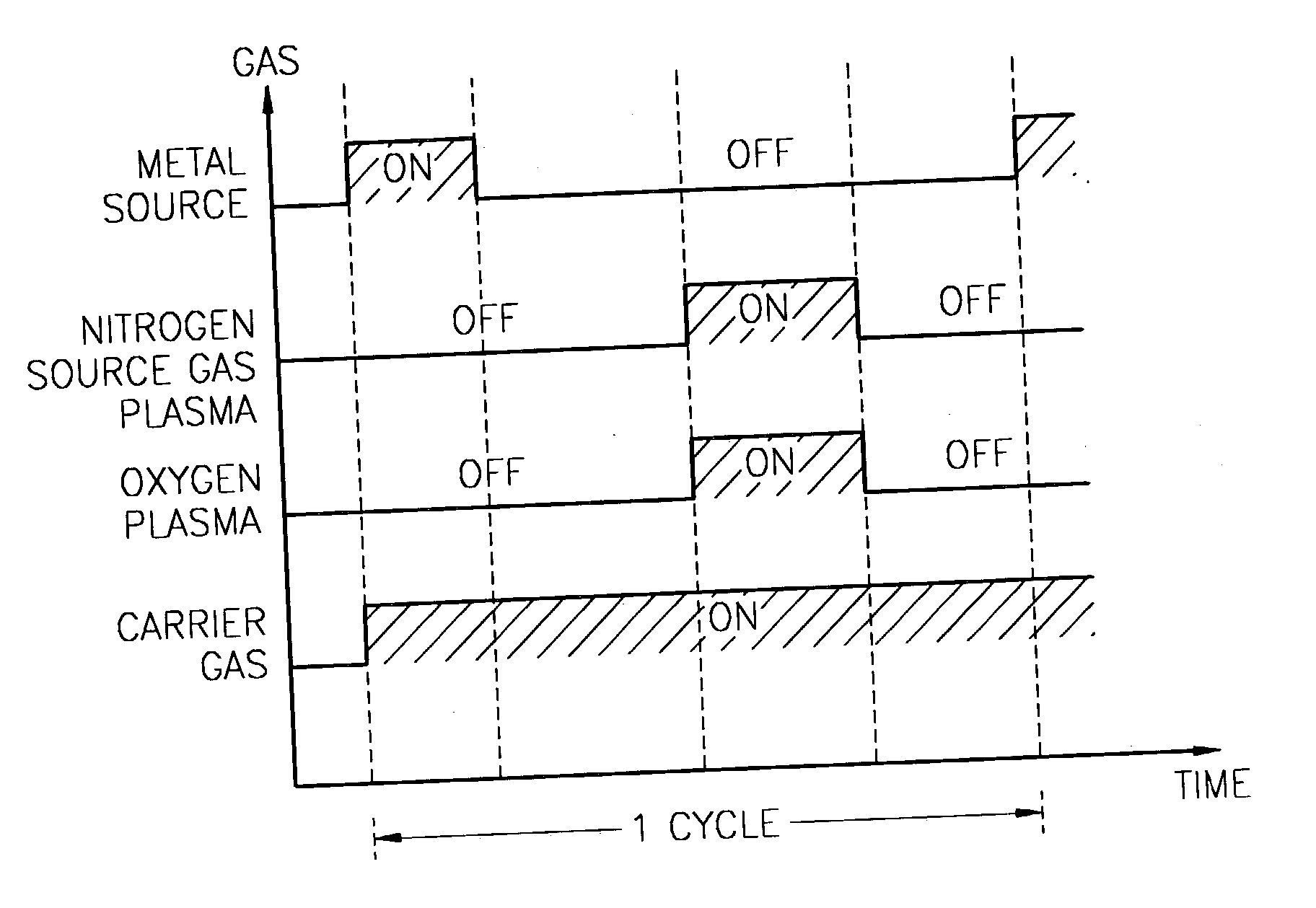
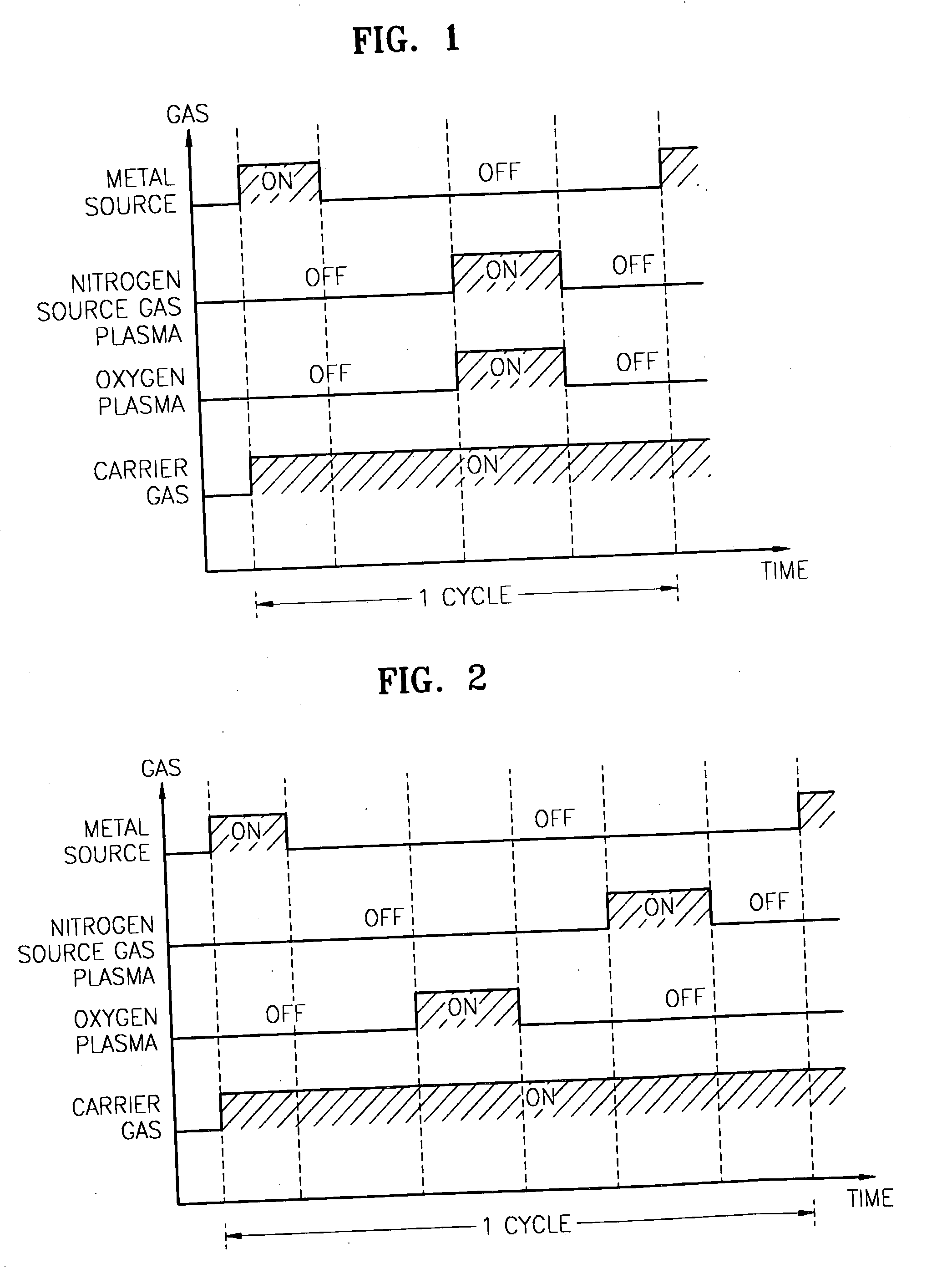
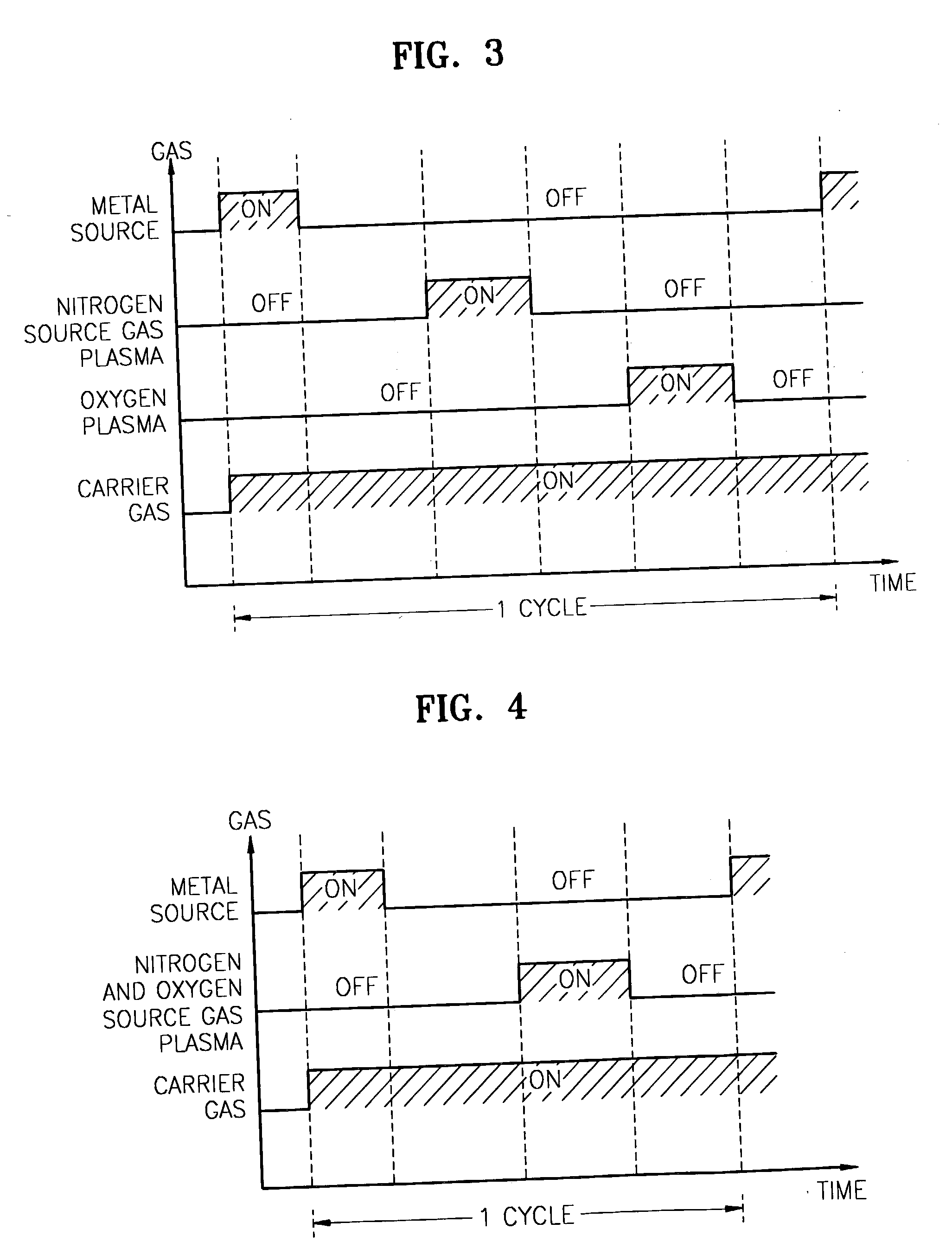
[0042] In order to verify the improved breakdown characteristics of the nitrogen-containing metal oxide thin film according to the present invention, a nitrogen-containing Al.sub.2O.sub.3 thin film was grown using PEALD. For comparison, Al.sub.2O.sub.3 thin films containing no nitrogen were grown by ALD and PEALD, respectively. The results are shown in FIGS. 8 and 9.

[0043] The nitrogen-containing Al.sub.2O.sub.3 thin film according to the present invention was deposited under the following experimental conditions. TMA was used as a metal source compound. Argon gas was flowed at a rate of 200 sccm to carry TMA while maintaining the total flow rate to 600 sccm. The process was performed at an oxygen flow rate of 50 sccm, a nitrogen gas flow rate of 5-10 sccm, an RF source power of 300 W, a reactor pressure of 3 torr, and a temperature of 250-300.degree. C. One cycle period was controlled to 6-7 seconds, and oxygen gas and nitrogen gas were simultaneously supplied according to the gas ...


PUM

PropertyMeasurementUnit
pressureaaaaaaaaaa
temperatureaaaaaaaaaa
thicknessaaaaaaaaaa

Abstract

A method for forming a nitrogen-containing oxide thin film by using plasma enhanced atomic layer deposition is provided. In the method, the nitrogen-containing oxide thin film is deposited by supplying a metal source compound and oxygen gas into a reactor in a cyclic fashion with sequential alternating pulses of the metal source compound and the oxygen gas, wherein the oxygen gas is activated into plasma in synchronization of the pulsing thereof, and a nitrogen source gas is further sequentially pulsed into the reactor and activated into plasma over the substrate in synchronization with the pulsing thereof. According to the method, a dense nitrogen-containing oxide thin film can be deposited at a high rate, and a trace of nitrogen atoms can be incorporated in situ into the nitrogen-containing oxide thin film, thereby increasing the breakdown voltage of the film.

Description

[0001] This application claims priority from Korean Patent Application No. 2002-64524, filed on Oct. 22, 2002, in the Korean Intellectual Property Office, the disclosure of which is incorporated herein in its entirety by reference.[0002] 1. Field of the Invention[0003] The present invention relates to a method for forming an insulating thin film in the manufacture of a variety of electronic devices, and more particularly, to a method for forming a metal oxide thin film using atomic layer deposition (ALD).[0004] 2. Description of the Related Art[0005] Generally, insulating films for electronic devices have been formed using physical vapor deposition (PVD) or chemical vapor deposition (CVD). Recently, the application of atomic layer deposition (ALD) in forming such insulating films is gradually increasing. As is well known, rather than simultaneously supplying source gases into a reactor, ALD involves sequentially alternating pulses of different kinds of source gases to form a thin fi...

Claims


Application Information

Patent Timeline
Patent Type & Authority Applications(United States)
IPC IPC(8): C23C16/30C23C16/44C23C16/455H01L21/20C23C16/50H01L21/314H01L21/316
CPCC23C16/308C23C16/45529H01L21/31616C23C16/50H01L21/3145C23C16/45542H01L21/02274H01L21/0228H01L21/02175H01L21/20
Inventor LIM, JUNG-WOOKYUN, SUN-JIN
Owner ELECTRONICS & TELECOMM RES INST
Why Eureka
Try Eureka