
Adhesive film for semiconductor, lead frame and semiconductor device using the same, and method of producing semiconductor device

a technology of adhesive film and lead frame, which is applied in the direction of film/foil adhesives without carriers, heat-activated film/foil adhesives, film/foil adhesives, etc., can solve the problems of sealing resin creeping even on the backside of lead frame, not enough area and thickness, and the sealing resin not being able to achieve the reduction in area and thickness. , to achieve the effect of easy peeling

Inactive Publication Date: 2004-07-01
RESONAC CORPORATION
View PDF9 Cites 10 Cited by
  • Summary
  • Abstract
  • Description
  • Claims
  • Application Information

AI Technical Summary

Benefits of technology

[0005] An object of the present invention is to provide an adhesive film for semiconductor and a lead frame and a semiconductor device using the same, which adhesive film not only has enough bonding strength to lead frames and, after resin sealing, can be easily peeled off, but also possesses other characteristics necessary in semiconductor applications.
[0006] Another object of the invention is to provide a method of producing semiconductor device whereby semiconductor devices of high density and small area and thickness can be produced efficiently.

Problems solved by technology

Some examples are LOC (lead on chip) and COL (chip on lead), but are not decreased enough in area and thickness.
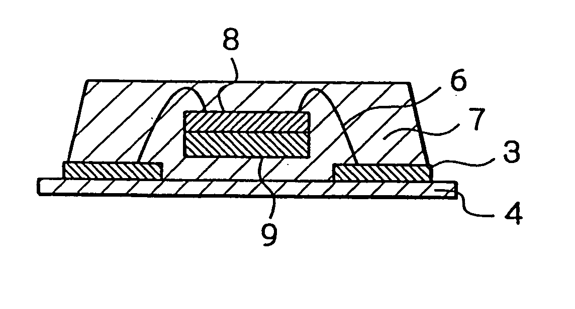
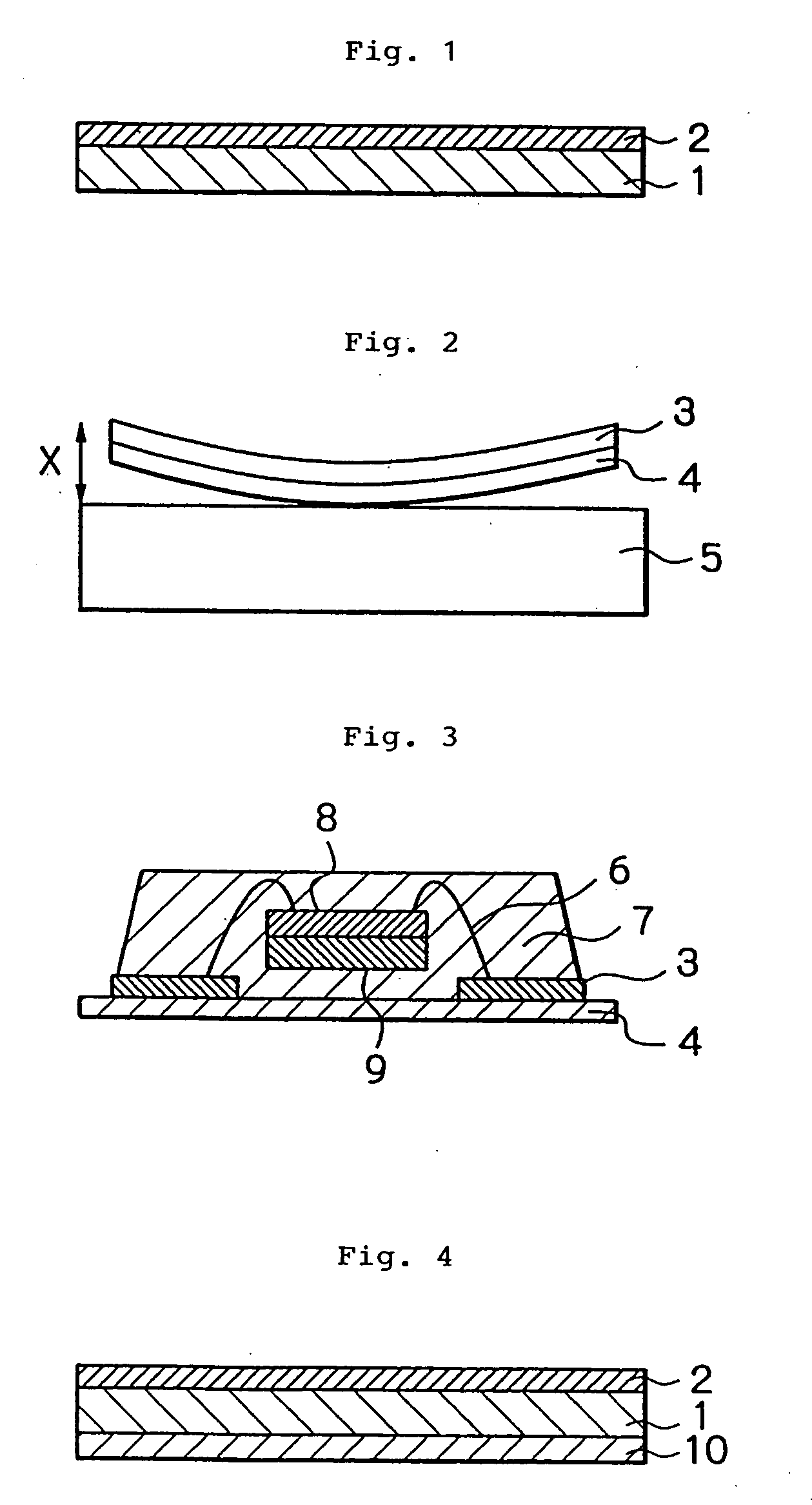
Packages of this structure achieve the decrease in area and thickness because lead frames do not protrude from sealing resin, but the sealing resin tends to creep even on the backside of lead frames.
However, there has been no adhesive film for semiconductor that possesses both the antipodal properties.

Method used


Image

  • Adhesive film for semiconductor, lead frame and semiconductor device using the same, and method of producing semiconductor device
  • Adhesive film for semiconductor, lead frame and semiconductor device using the same, and method of producing semiconductor device
  • Adhesive film for semiconductor, lead frame and semiconductor device using the same, and method of producing semiconductor device

Examples


preparation example 1

Preparation of the Aromatic Polyether Amideimide Adhesive Varnish Used in Examples 1-4, 7 and 8

[0118] Into a 5-liter four neck distillation flask equipped with a thermometer, a stirrer, a nitrogen inlet tube and a fractionating column were placed 258.3 g (0.63 mol) of 2,2-bis[4-(4-aminophenoxy)phenyl]propan-e and 10.4 g (0.042 mol) of 1,3-bis(3-aminopropyl)tetramethyldisiloxane, and dissolved in 1450 g of N-methyl-2-pyrrolidone. The solution was heated to 70.degree. C., and 33.6 g (0.168 mol) of 1,12-diaminododecane was dissolved therein. The solution was cooled to 0.degree. C., and 180.4 g (0.857 mol) of trimellitic anhydride chloride was added. After the trimellitic anhydride chloride was dissolved, 130 g of triethylamine was added. After stirring for 2 hours at room temperature, the temperature was raised to 180.degree. C. and reaction was carried out for 5 hours to complete imidation. The resulting reaction solution was poured in methanol to separate a polymer. After dried, the ...

preparation example 2

Preparation of the Aromatic Polyether Amideimide Adhesive Varnish Used in Examples 5 and 6

[0119] Into a 5-liter four neck distillation flask equipped with a thermometer, a stirrer, a nitrogen inlet tube and a fractionating column were placed 258.6 g (0.63 mol) of 2,2-bis[4-(4-aminophenoxy)phenyl]propan-e and 67.0 g (0.27 mol) of 1,3-bis(3-aminopropyl)tetramethyldisiloxane, and dissolved in 1550 g of N-methyl-2-pyrrolidone. The solution was cooled to 0.degree. C., and 187.3 g (0.89 mol) of trimellitic anhydride chloride was added at the same temperature. After the trimellitic anhydride chloride was dissolved, 100 g of triethylamine was added. After stirring for 2 hours at room temperature, the temperature was raised to 180.degree. C. and reaction was carried out for 5 hours to complete imidation. The resulting reaction solution was poured in methanol to separate a polymer. After dried, the polymer was dissolved in N-methyl-2-pyrrolidone, and separated again in methanol. Drying under ...

preparation example 3

Preparation of the Aromatic Polyether Amideimide Varnish Used for Forming a Resin Layer B in Example 5

[0120] Into a 5-liter four neck distillation flask equipped with a thermometer, a stirrer, a nitrogen inlet tube and a fractionating column were placed 172.4 g (0.42 mol) of 2,2-bis[4-(4-aminophenoxy)phenyl]propan-e and 153.7 g (0.42 mol) of 4,4'-methylene-bis(2,6-diisopropylaniline), and dissolved in 1550 g of N-methyl-2-pyrrolidone. The solution was cooled to 0.degree. C., and 174.7 g (0.83 mol) of trimellitic anhydride chloride was added at the same temperature. After the trimellitic anhydride chloride was dissolved, 130 g of triethylamine was added. After stirring for 2 hours at room temperature, the temperature was raised to 180.degree. C. and reaction was carried out for 5 hours to complete imidation. The resulting reaction solution was poured in methanol to separate a polymer. After dried, the polymer was dissolved in N-methyl-2-pyrrolidone, and separated again in methanol. D...


PUM

PropertyMeasurementUnit
thicknessaaaaaaaaaa
glass transition temperatureaaaaaaaaaa
90°-peel strengthaaaaaaaaaa

Abstract

An adhesive film for semiconductor, which comprises at least one resin layer, and, after bonded to a lead frame, has at 25° C. a 90°-peel strength of at least 5 N / m between the resin layer and the lead frame, and, after a lead frame is bonded to the adhesive film for semiconductor and sealed with a sealing material, has at least at one point of temperatures ranging from 0 to 250° C a 90°-peel strength of at most 1000 N / m between the resin layer and each of the lead frame and the sealing material; a lead frame and a semiconductor device using the adhesive film for semiconductor; and a method of producing a semiconductor device.

Description

[0001] The present invention relates to an adhesive film for semiconductor, a lead frame and a semiconductor device using the adhesive film for semiconductor, which adhesive film can be easily peeled off from lead frames and sealing resins, contributing to high working efficiency in the production of packaged semiconductor devices. The present invention also relates to a method of producing a semiconductor device.[0002] Conventional packaged semiconductor devices have been produced by bonding a semiconductor element to a die pad of a lead frame with an adhesive such as a silver paste, connecting it with the lead frame by wire-bonding and then sealing the whole body except outer leads for external connection. However, with a recent demand for packaged semiconductor devices of higher density and smaller area and thickness, packages of various structures have been developed. Some examples are LOC (lead on chip) and COL (chip on lead), but are not decreased enough in area and thickness....

Claims


Application Information

Patent Timeline
Patent Type & Authority Applications(United States)
IPC IPC(8): H01L21/60C09J7/10C09J7/22C09J7/35H01L21/52H01L21/56H01L21/68H01L23/31H01L23/48H01L23/495
CPCC09J7/00Y10T428/28C09J177/00C09J179/08C09J2461/006C09J2467/006C09J2477/006C09J2479/08C09J2479/086C09J2481/006H01L21/56H01L21/568H01L21/6835H01L23/3107H01L23/49513H01L24/83H01L24/97H01L2224/48247H01L2224/83801H01L2224/97H01L2924/01004H01L2924/01013H01L2924/01015H01L2924/01027H01L2924/01029H01L2924/01033H01L2924/0104H01L2924/01046H01L2924/01047H01L2924/01058H01L2924/01078H01L2924/01079H01L2924/01082H01L2924/09701H01L2924/3511C09J7/0242Y10T428/1471Y10T428/1476H01L2924/15747H01L2224/48091H01L2224/45144H01L2924/01006H01L2924/01005H01L24/48H01L2224/85H01L2924/3512H01L2924/00H01L2924/00014H01L2924/181H01L24/45C09J7/35C09J7/10C09J2203/326H01L2924/00012H01L21/52H01L21/60C09J7/22
Inventor KAWAI, TOSHIYASUMATSUURA, HIDEKAZU
Owner RESONAC CORPORATION
Learn More