

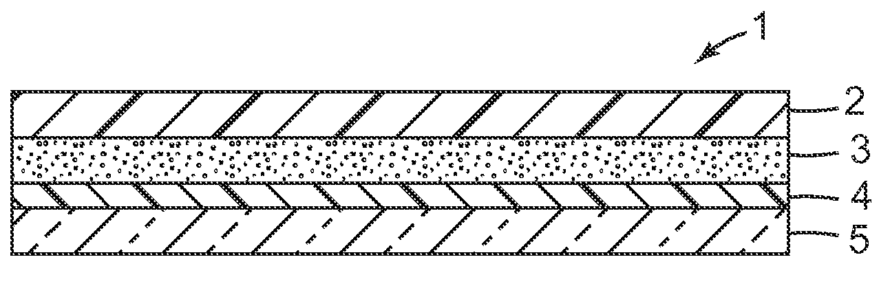
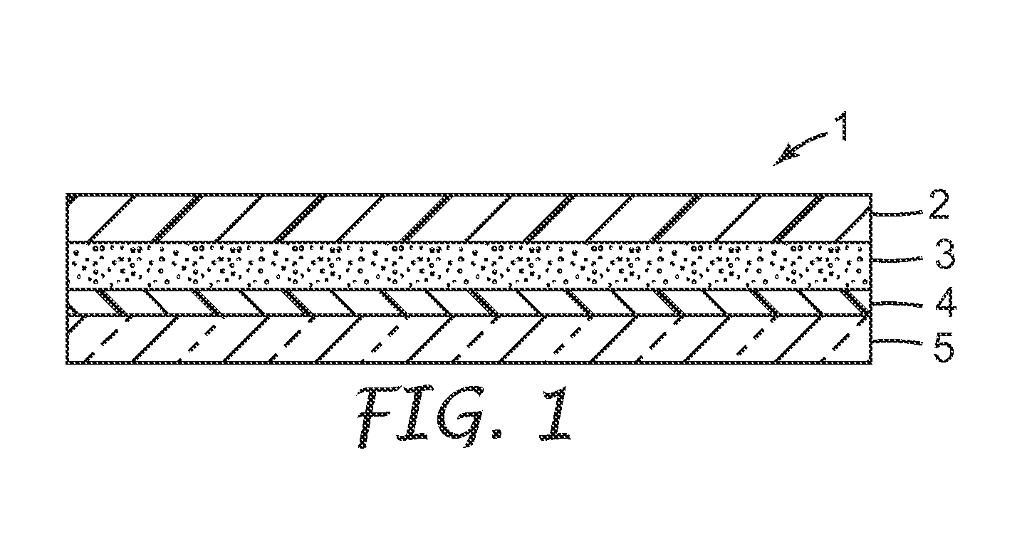
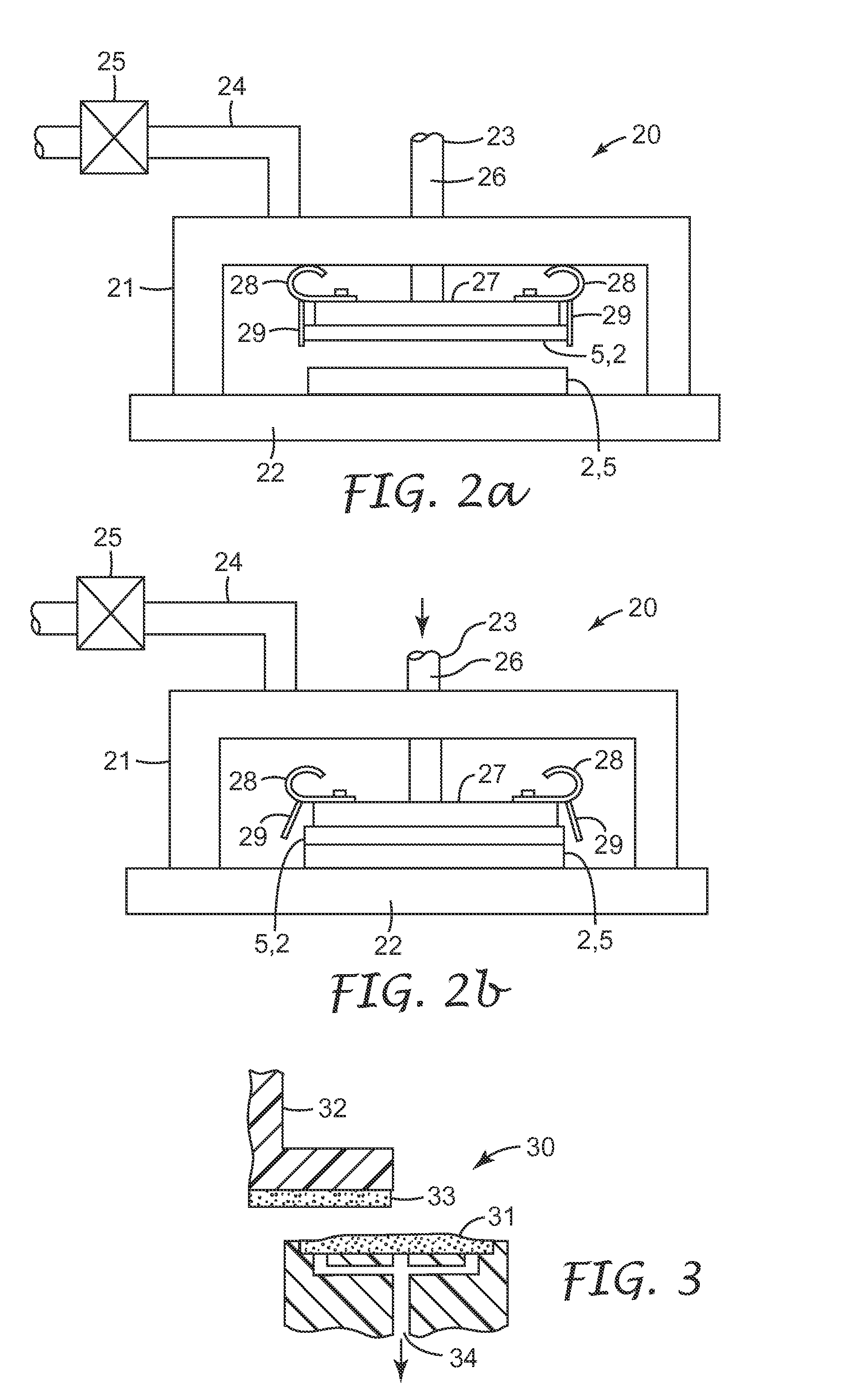
Layered body and method for manufacturing thin substrate using the layered body
- Summary
- Abstract
- Description
- Claims
- Application Information
AI Technical Summary
Benefits of technology
Problems solved by technology
Method used
Image

Examples
examples
[0089]These examples are merely for illustrative purposes only and are not meant to be limiting on the scope of the claims. All parts, percentages, ratios, etc. in the examples and the rest of the specification are by weight, unless noted otherwise.
[0090]Table 1 shows the formulation components and trade names that were used in the following examples. The following formulation components do not constitute an exclusive list, but should be interpreted only in light of the comparative examples for which they were used. Those skilled in the art will understand other formulation components may also correspond to a reasonable interpretation of the claims.
Formulation Components
[0091]
TABLE 1Abbreviation orTradeDesignationDescriptionRicacryl 3500Methacrylated polybutadiene commercially availablefrom Sartomer, Exton, PASR 238Hexanediol diacrylate commercially available fromSartomer, Exton, PACN 117Modified epoxy acrylate commercially available fromSartomer, Exton, PASR 349Ethoxylated (3) bisp...
PUM
| Property | Measurement | Unit |
|---|---|---|
| Fraction | aaaaa | aaaaa |
| Fraction | aaaaa | aaaaa |
| Percent by mass | aaaaa | aaaaa |
Abstract
Description
Claims
Application Information