Signal transmission plate used in an assembly package

a technology of signal transmission plate and assembly package, which is applied in the direction of electrical equipment, semiconductor devices, semiconductor/solid-state device details, etc., can solve the problems of reducing the signal transmission quality, increasing the transmission distance, and affecting the signal transmission quality of the di

Inactive Publication Date: 2004-07-29
YANG CHAUR CHIN
View PDF9 Cites 0 Cited by
  • Summary
  • Abstract
  • Description
  • Claims
  • Application Information

AI Technical Summary

Benefits of technology

[0011] The assembly package of the invention employs flip-chip bonding, so that the signals from the first die (the bottom die) are transmitted to the substrate. Therefore, imperfect electricity caused by using lead connection is prevented. Also, the second die also utilizes flip-chip bonding so that the signals are transmitted to the signal transmission plate and then to the substrate via the conductive wires. As a result, the conductive wires are not required to connect to the joints on the top die; only the signal transmission plate is needed to connect with the wire bonding pads, and signals from the top die can be transmitted to the substrate. In other words, the signal transmission quality is improved, and the signal transmission rate is also increased, for that the transmission distance of the conductive wires is shortened.

Problems solved by technology

Nevertheless, by using conductive wires to electrically connect I / O pins of individual die with the substrate for signal transmission, the signal transmission quality of the die may be affected by the transmission distance and the number of conductive wires.
However, the longer the transmission distance of conductive wires gets, the noise increases accordingly, and the signal distortion and hysteresis become more apparent, thereby dropping the signal transmission quality.

Method used


Image

  • Signal transmission plate used in an assembly package
  • Signal transmission plate used in an assembly package
  • Signal transmission plate used in an assembly package

Examples


Embodiment Construction

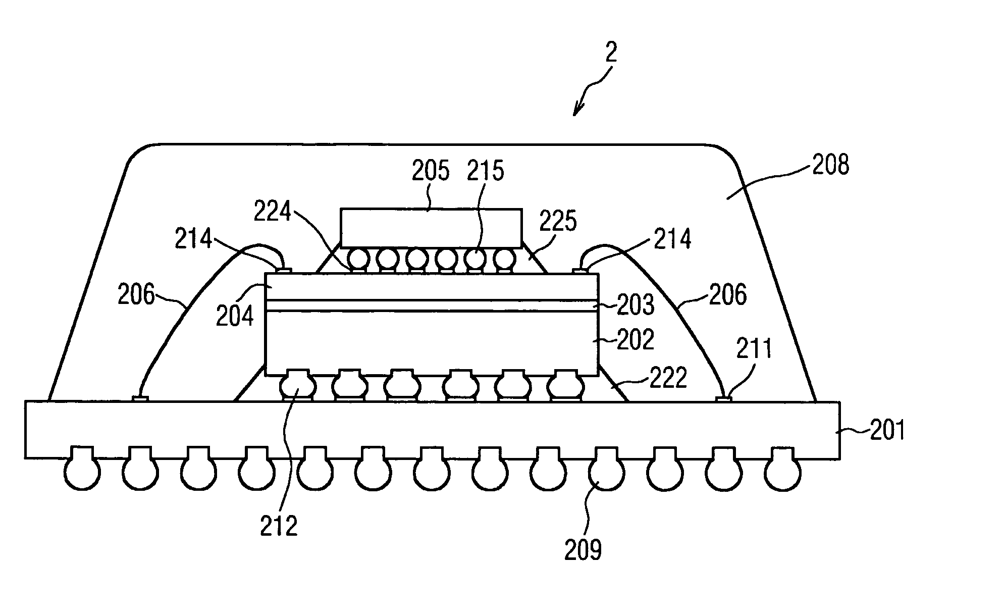
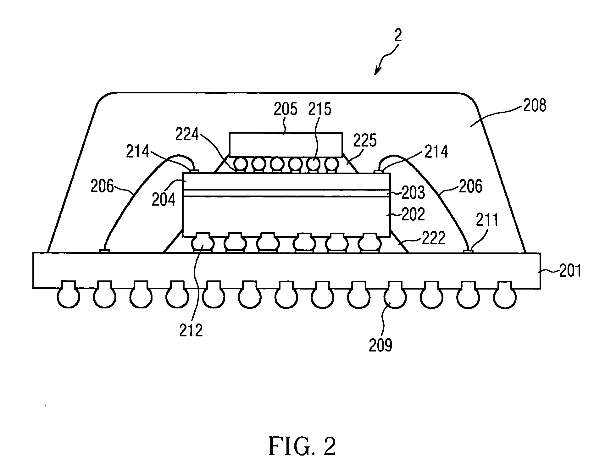
[0016] The assembly package of the invention will be described with reference to the accompanying drawings.

[0017] Referring to FIG. 2, an assembly package 2 of the invention includes a first die 202, a signal transmission plate 204, a second die 205, and a plurality of conductive wires 206. The first die 202 is provided with a plurality of first bumps 212, solder bumps for instance, which are electrically connected with a substrate 201 using flip-chip bonding. Between the substrate 201 and the first die 202 is an underfill 222 to prevent the stress concentration brought about by different thermal expansion coefficients of the substrate 201 and the first die 202.

[0018] The signal transmission plate 204 is fixed onto the first die 202 by using an adhesive 203, for example, silver paste or non-conductive materials such as epoxy. Referring to FIG. 3, the signal transmission plate 204 includes an insulating layer 214, a layout wire layer 224, and a solder mask layer 234. The insulating l...


PUM


Abstract

A signal transmission plate used in an assembly package includes at least one insulating layer, at least one layout wire layer formed on the insulating layer, and a solder mask layer formed on the layout wire layer. The solder mask layer exposes partial area of the layout wire layer at the center and peripheries of the signal transmission plate to form a plurality of die bonding pads and a plurality of wire bonding pads.

Description

[0001] This is a Divisional application claiming priority under 35 U.S.C. .sctn.120, of co-pending prior application Ser. No. 10 / 293,123 filed on Nov. 12, 2002, the disclosure of which is incorporated herein by reference.[0002] 1. Field of the Invention[0003] The invention relates to a signal transmission plate used in an assembly package.[0004] 2. Description of the Related Art[0005] During the recent years, due to the steady increase of demand of consumer electronic products, namely, cellular phones, personal digital assistants (PDAs) and digital cameras, package structures are developed toward being light in weight and small in size with short signal transmission distances. Based upon such trend, in order to save package area as well as to improve problems such as signal distortion, delay or power loss, an assembly package integrates at least one die into a same package structure by perpendicular stacking.[0006] Referring to FIG. 1, a conventional ball grid array (BGA) package 1 ...

Claims


Application Information

Patent Timeline
Patent Type & Authority Applications(United States)
IPC IPC(8): H01L21/56H01L23/31H01L25/065
CPCH01L21/563H01L23/3128H01L2224/73204H01L2224/32225H01L2224/16225H01L2924/07802H01L2224/45144H01L2924/01087H01L24/48H01L2924/3011H01L2924/15311H01L2924/01079H01L2225/06586H01L2225/06582H01L2225/06517H01L2225/06513H01L2225/0651H01L2224/73265H01L2224/73253H01L2224/73215H01L2224/73207H01L2224/73203H01L2224/48227H01L2224/48091H01L2224/32145H01L2224/16145H01L25/0657H01L2924/00014H01L2924/00H01L24/45H01L2924/181H01L2924/00015H01L2224/05599H01L2924/00012
Inventor YANG, CHAUR-CHIN
Owner YANG CHAUR CHIN
Why Eureka
Try Eureka