Method of manufacturing electronic part, electronic part, method of mounting electronic part, and electronic apparatus

a technology of electronic components and mounting methods, applied in the direction of electrical permutation locks, lock applications, coatings, etc., can solve the problems of inability to electrically connect the counterpart substrate, the inability to use unused adhesive conductive particles 298, and the inability to use expensive conductive particles for all electrical connections

Active Publication Date: 2004-11-11
BOE TECH GRP CO LTD
View PDF4 Cites 34 Cited by
  • Summary
  • Abstract
  • Description
  • Claims
  • Application Information

AI Technical Summary

Problems solved by technology

Also, the expensive conductive particles cannot be used for all of the electrical connection.
However, in the mounting method disclosed in the Japanese Unexamined Patent Application Publication No. 2002-170837, since the adhesive conductive particles 298 fixed on the surface of the resist film 280 are removed together with the resist film 280 as mentioned above, it has a disadvantage in that the unused adhesive conductive particles 298 cannot be used again.
Thereby it has a problem that it is impossible to electrically connect the counterpart substrate 220 with the electronic part 270.

Method used


Image

  • Method of manufacturing electronic part, electronic part, method of mounting electronic part, and electronic apparatus
  • Method of manufacturing electronic part, electronic part, method of mounting electronic part, and electronic apparatus
  • Method of manufacturing electronic part, electronic part, method of mounting electronic part, and electronic apparatus

Examples


Embodiment Construction

[0073] Hereinafter, the exemplary embodiments of the present invention will be described in detail with reference to the drawings. Also, each element in the drawings is changed to appropriate scale such that it is legible.

Liquid Crystal Display Device

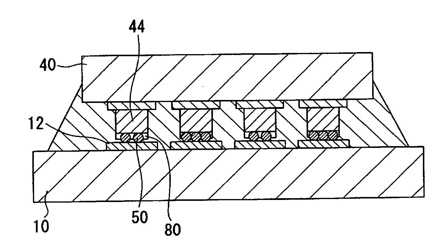
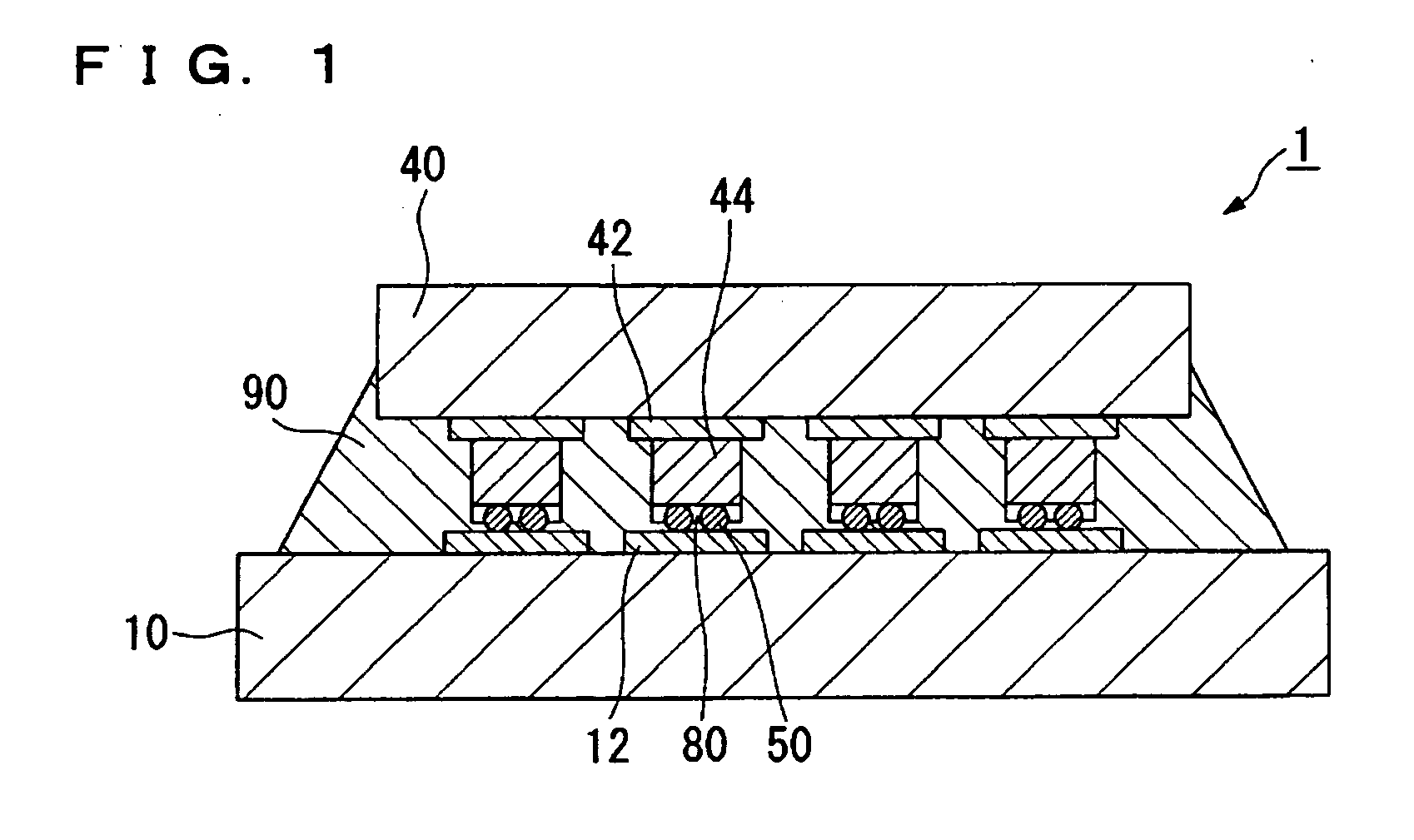
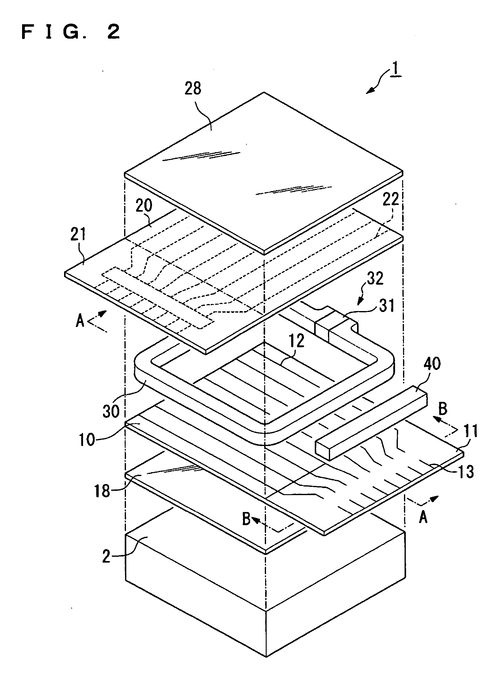
[0074] First, a liquid crystal display device using IC, an exemplary embodiment of the electronic part according to the present invention, will be explained below with reference to FIGS. 2 and 3. Also, FIG. 2 is an exploded perspective view of a liquid crystal display device, and FIG. 3 is a side sectional view along plane A-A of FIG. 2. Also, even though an aspect of the present invention is explained based on a passive matrix type liquid crystal display device as an exemplary embodiment thereof, it can be also adopted to an active matrix type liquid crystal display device.

[0075] As shown in FIG. 2, in the liquid crystal display device 1 as an exemplary embodiment of the present invention, a set of lower substrate 10 and upper substrat...


PUM


Abstract

To provide a method of manufacturing an electronic part capable of reusing the remaining conductive particles and electrically connecting the electronic part to the counterpart substrate, a method of manufacturing an electronic part includes: forming a mask on an active surface of the wafer on which electrode pads of the electronic part are formed, the mask of a predetermined height having openings provided above the electrode pads, forming bumps inside of the openings of the mask provided above the electrode pads, the bumps having a height lower than that of the mask, scattering conductive particles above the active surface of the wafer, removing the conductive particles remaining on the surface of the mask, fixing the conductive particles on the surfaces of the bumps, removing the mask, and separating the electronic part from the wafer.

Description

[0001] 1. Field of Invention[0002] The present invention relates to a method of manufacturing an electronic part, the electronic part manufactured according to the method, a method of mounting the electronic part, and an electronic apparatus.[0003] 2. Description of Related Art[0004] Electronic parts, such as an IC, etc. are mounted onto a circuit board etc. for use. Various methods are proposed to mount the electronic part onto the circuit board. FIG. 9 shows a view for explaining a method of mounting the electronic part according to the related art. As shown in FIG. 9(A), the electronic part 170, such as the IC, etc. is mounted onto the counterpart substrate 120 while interposing an anisotropic conductive film (ACF) 190 therebetween. Conductive particles 195 distributed in a thermosetting resin 192 form the anisotropic conductive film 190. The conductive particles 195 are interposed between the electrode pad 172 formed on the active surface of the electronic part 170 and the elect...

Claims


Application Information

Patent Timeline
Patent Type & Authority Applications(United States)
IPC IPC(8): H01L21/56H01L21/60H01L23/485
CPCH01L21/563H01L2224/11332H01L24/12H01L2224/1147H01L2224/11901H01L2224/13099H01L2224/16225H01L2224/73204H01L2224/83192H01L2924/01004H01L2924/01013H01L2924/0103H01L2924/01033H01L2924/01049H01L2924/01078H01L2924/01079H01L2924/14H01L2924/3025H01L2924/01005H01L2924/01006H01L2924/014H01L24/83H01L2224/32225H01L24/11H01L2924/00H01L2224/05573H01L2224/05568H01L2224/05624H01L2924/00014E05B47/026E05B49/00E05B2047/002
Inventor SAITO, ATSUSHI
Owner BOE TECH GRP CO LTD
Why Eureka
Try Eureka