Surface-mount-enhanced lead frame and method for fabricating semiconductor package with the same

a technology of lead frame and surface mount, which is applied in the direction of printed circuit, sustainable manufacturing/processing, final product manufacturing, etc., can solve the problems of poor wettability and adhesion between the semiconductor package and the printed circuit board, further affecting the reliability of the semiconductor device, and increasing the product siz

Inactive Publication Date: 2004-12-02
SILICONWARE PRECISION IND CO LTD
View PDF7 Cites 36 Cited by
  • Summary
  • Abstract
  • Description
  • Claims
  • Application Information

AI Technical Summary

Problems solved by technology

It thus causes poor wettability and adhesion between the semiconductor package and the printed circuit board.
Solder joints of the leads 12 and the printed circuit board may be separated due to bad joints or solder openings, since the surfaces of the leads may wet with insufficient tin.
This causes unreliable signal transmission and further affects the reliability of the semiconductor devices.
However, in this manner, the product size is increased, unfavorable to the miniaturization requirements of semiconductor devices.
In addition, special mold is needed to bend the externally exposed leads into bent shapes, this not only increases the material costs, but also the chances of poor quality of the bent part such as the peeling off of the bent part.

Method used


Image

  • Surface-mount-enhanced lead frame and method for fabricating semiconductor package with the same
  • Surface-mount-enhanced lead frame and method for fabricating semiconductor package with the same
  • Surface-mount-enhanced lead frame and method for fabricating semiconductor package with the same

Examples


Embodiment Construction

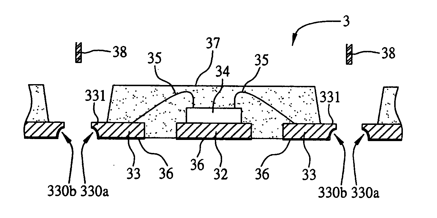
[0024] Lead frame suitable for quad-flat non-leaded (QFN) package is disclosed in detail in the embodiments of the present invention below. The embodiments of the present invention are provided to illustrate the lead frame suitable for QFN package, thought the lead frame disclosed in the present invention is not limited to this.

[0025] Referring to FIG. 3A and FIG. 3B, they are the schematics of the surface-mount-enhanced lead frame of the present invention, however these diagrams are simplified schematics illustratively showing the structural units related to the present invention, the actual lead frame and the semiconductor package layout are more complicated.

[0026] The surface-mount-enhanced lead frame 31 of the present invention consists mainly of a die pad 32 and a plurality of leads 33 distributed around the die pad 32, and a dam bar structure 331 formed with an indentation 330 is connected to the end of the leads 33 away from the die pad 32.

[0027] The die pad 32 is connected t...


PUM


Abstract

A surface-mount-enhanced lead frame and a method for fabricating a semiconductor package with the lead frame are proposed, wherein a dam bar structure between any two neighboring lead frames of a lead frame module plate is formed with an indentation and at least a solder metal layer is applied on the bottom surface of the lead frame and the indentation. A singulation process is performed along the indentation to separate the lead frame module plate mounted with semiconductor chips and package body into a plurality of packages. Therefore, the indentation and the solder metal layer applied thereon can provide solder paste improved wettability and increased solder surface, while the semiconductor package with the lead frame is mounted on an external device via a surface-mount-technology, so as to prevent problems of signal transmission owing to separation of solder joint from solder open.

Description

[0001] The present invention relates to a surface-mount-enhanced lead frame and a method for fabricating the semiconductor package with the same, and in particular, relates to a quad-flat non-leaded (QFN) lead frame structure and the semiconductor package utilizing the lead frame and its manufacturing processes.DESCRIPTION OF THE PRIOR ART[0002] Conventional semiconductor packages use lead frames as die pads to enable the formation of semiconductor packages. The lead frame typically comprises a die pad and a plurality of leads formed around the die pad. After the semiconductor chip is bonded on the die pad and electrically connected to the leads via bonding wires, the chip, die pad, bonding wires and the inner part of the leads are encapsulated by a package body to form the semiconductor package with the lead frame.[0003] There are various structures and types of semiconductor packages using a lead frame as the chip carrier, for example, a quad-flat package (QFP), a quad-flat non-le...

Claims


Application Information

Patent Timeline
Patent Type & Authority Applications(United States)
IPC IPC(8): H01L23/31H01L23/495H05K3/34
CPCH01L23/3107H01L23/49548H01L2224/45144H01L2924/01033H01L24/49H01L24/48H05K2201/1084H05K2201/10689H05K3/3426H01L2924/01082H01L24/97H01L2224/48091H01L2224/48247H01L2224/49171H01L2224/97H01L2924/01029H01L2924/01046H01L2924/01079H01L2224/85H01L2924/00014H01L2924/00H01L24/45H01L2924/181Y02P70/50H01L2924/18301H01L2924/00015H01L2224/05599H01L2924/00012
Inventor LEE, TE-HAWCHENG, KAUN-ICHANG, YUEH-CHIUNGLIU, SHIH-YAOHUANG, KUN-MING
Owner SILICONWARE PRECISION IND CO LTD
Why Eureka
Try Eureka