

LCD device having a smaller level difference
a level difference, liquid crystal display technology, applied in non-linear optics, instruments, optics, etc., can solve the problems of affecting the image quality and affecting the level difference of the lcd devi
- Summary
- Abstract
- Description
- Claims
- Application Information
AI Technical Summary
Benefits of technology
Problems solved by technology
Method used
Image

Examples
first embodiment
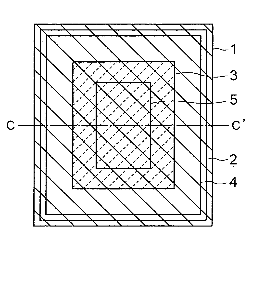
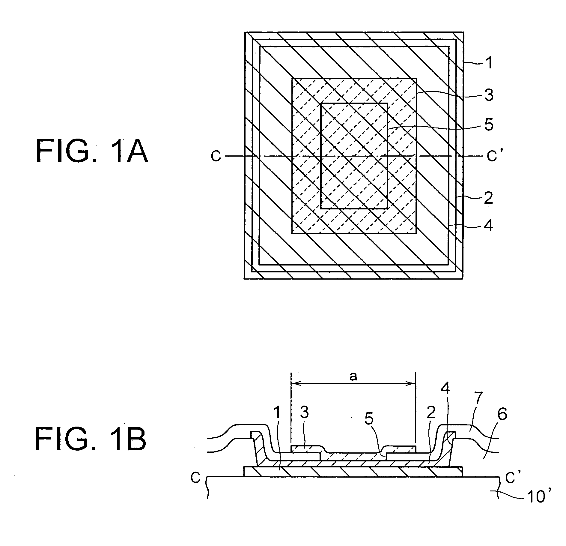
[0033] Referring to FIGS. 1A and 1B, there is shown the structure of a scanning terminal in an LCD device according to the present invention. The LCD device shown in these figures is an AM-LCD device, the overall configuration thereof being similar to that shown in FIG. 3. More specifically, as shown in FIG. 3, the LCD device of the present embodiment includes a TFT substrate 11 and a counter substrate 12 sandwiching therebetween an LC layer.
[0034] The TFT substrate 11 mounts thereon a plurality of signal lines 13 extending parallel to one another, and a plurality of scanning lines 14 extending perpendicular to the signal lines 13. A plurality of pixel electrodes 17 each associated with a TFT 18 are disposed in a matrix at the intersections between the signal lines 13 and the scanning lines 14.
[0035] At the ends of the signal lines 13, there are provided respective signal terminals 16, whereas there are provided scanning terminals 15 at the ends of the respective scanning lines 14. ...
second embodiment
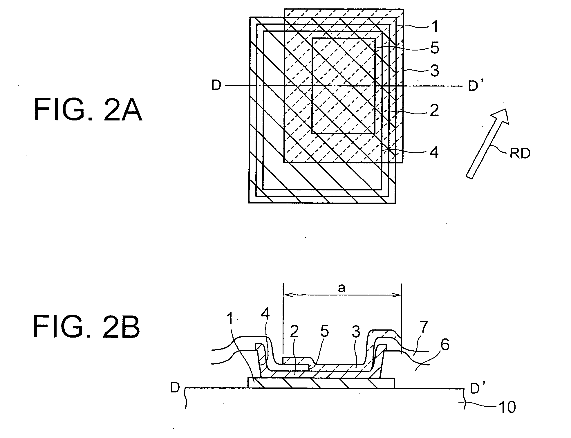
[0045] Referring to FIGS. 2A and 2B, there is shown the structure of the vicinity of a terminal in an LCD device according to the present invention. The rubbing direction of the orientation film is shown by an arrow RD, which is directed from the bottom left to the top right, as viewed in FIG. 2A. The terminal shown in FIGS. 2A and 2B is similar to the terminal shown in FIGS. 1A and 1B except that the center of the second via hole 5 is deviated from the center of the first via hole 4 in the direction RD of the rubbing treatment, and that the ITO film pattern 3 is formed in the second via hole 5 and has four edges overlying the four edges of the second dielectric film 7 constituting the second via hole 5.
[0046] The ITO film patterns 3 are disposed to correspond to the pattern and pitch of the terminals of the driving circuit. The second via hole 5 is located within the area of the ITO film pattern 3. In addition, the leading edge of the first metallic film pattern 1, the leading peri...
PUM
 Abstract
Description
Claims
Application Information