Semiconductor light-emitting device

a technology of semiconductors and light-emitting devices, which is applied in the direction of solid-state devices, basic electric elements, transportation and packaging, etc., can solve the problems of insufficient external quantum efficiency, achieve the effect of improving the utilization efficiency of light, improving the output power of devices, and improving the efficiency of light utilization

Inactive Publication Date: 2005-01-06
NICHIA CORP
View PDF58 Cites 134 Cited by
  • Summary
  • Abstract
  • Description
  • Claims
  • Application Information

AI Technical Summary

Benefits of technology

[0009] Therefore, an object of the present invention is to provide a semiconductor light emitting device wherein an improved external quantum efficiency can be stably secured.
[0028] In the case of the gallium nitride semiconductor, including a semiconductor having at least gallium and nitrogen, a portion near the peripheral of the p-side electrode, which is formed on the p-type semiconductor layer, lights brighter than other portions. By forming openings in the electrode, not only the light absorption is decreased, but also the length of the peripheral of the p-side electrode, where the light strongly emits, is increased. Therefore, the efficiency of the light utilization is improved. It is preferable for L / S≧0.024 μm / μm2 to be fulfilled wherein the total area of the ohmic electrode including the openings is S and the total sum of the length of the inner periphery of the openings is L. This improves the efficiency of the light utilization, by increasing the length of the peripheral of the electrode.

Problems solved by technology

In addition, if the light absorption within the light guide is so large, the external quantum efficiency does not reach a sufficient level only with the randomly roughed surface.

Method used


Image

  • Semiconductor light-emitting device
  • Semiconductor light-emitting device
  • Semiconductor light-emitting device

Examples


example 1

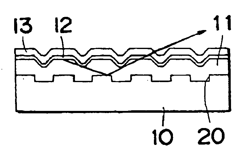
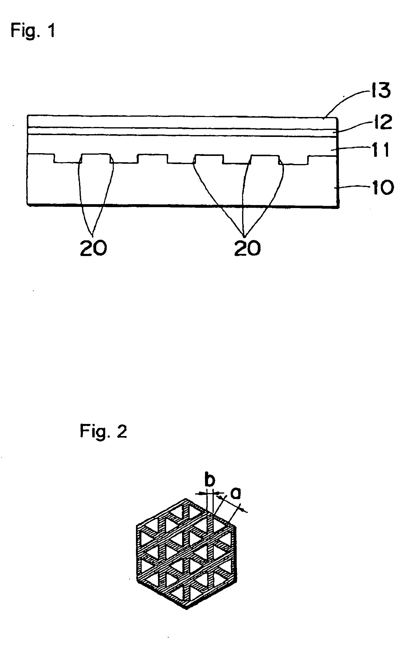
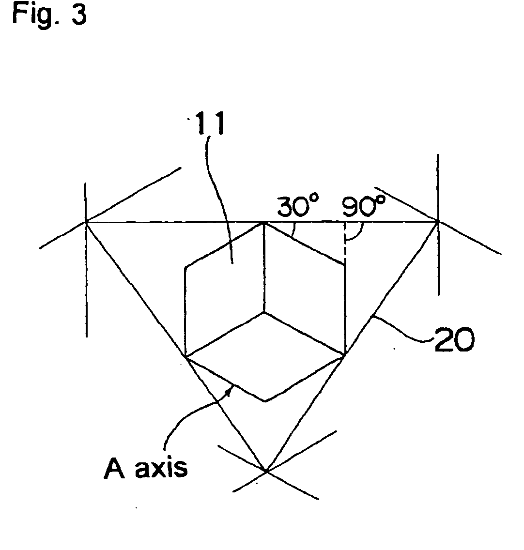
[0100] A sapphire substrate, of which a C plane (0001) is used as the main surface, having the orientation flat in an A plane (11-20), is used as the substrate.

[0101] First, an SiO2 film 30 that becomes an etching mask is formed on a sapphire substrate 10, as shown in FIG. 4A.

[0102] Next, a photomask of an equilateral triangle having a side of 5 μm is utilized and the photomask is arranged so that one side of the equilateral triangle becomes perpendicular to the orientation flat while the respective sides of the equilateral triangle become approximately parallel to (1-100), (01-10) and (-1010), that is to say, an M plane and then, after SiO2 film 30 and sapphire substrate 10 are etched by 3 μm to 4 μm using RIE, as shown in FIGS. 4B and 4C, a repeating pattern of protruding portions 20 (hatched areas are unetched areas, that is to say, protruding portions), as shown in FIG. 11B, is formed in the surface portion of sapphire substrate 10 when SiO2 film 30 is removed. As for the leng...

example 2

[0110] A sapphire substrate, of which a C plane (0001) is used as the main surface, having the orientation flat in an A plane (11-20) is used as the substrate.

[0111] A process in the substrate and layering of an n-type semiconductor layer to a p-type semiconductor layer are carried out in the same manner as in first example.

[0112] Next, a p-type semiconductor layer made of Mg doped GaN, an active layer and a portion of the n-type semiconductor layer are etched in order to form an n electrode so that the n-type semiconductor layer made of Si doped GaN is exposed.

[0113] Next, a photomask having a pattern wherein equilateral triangles having a side of 5 μm, as shown in FIG. 16, are most densely filled per unit area is utilized so that a light transmitting p electrode made of Ni / Au is formed on almost the entirety of the surface of the p-type semiconductor layer.

[0114] Furthermore, a p-side pad electrode made of Au is formed at a position opposite to the exposed surface of the n-typ...

example 3

[0117] A sapphire substrate, of which a C plane (0001) is used as the main surface, having the orientation flat in an A plane (11-20) is used as the substrate.

[0118] A process of the substrate and layering of an n-type semiconductor layer to a p-type semiconductor layer are carried out in the same manner as in first example.

[0119] Next, starting from Mg doped GaN, the p-type semiconductor layer, an active layer and a portion of the n-type semiconductor layer are etched in order to form an n electrode so that the Si doped GaN layer is exposed.

[0120] Next, a photomask of a square pattern is utilized so as to form a p electrode 104 made of Rh on almost the entirety of the surface of the p-type semiconductor layer. The shape of the openings is square, of which side is 7.7 μm. The interval of the openings is 6.3 μm. The aperture ratio of the opening is about 30%.

[0121] Furthermore, a p-side pad electrode made of Pt / Au is formed at a position opposite to the exposed surface of the n-t...


PUM


Abstract

A high external quantum efficiency is stably secured in a semiconductor light emitting device. At least one recess and / or protruding portion is created on the surface portion of a substrate for scattering or diffracting light generated in a light emitting region. The recess and / or protruding portion has a shape that prevents crystal defects from occurring in semiconductor layers.

Description

FIELD OF THE INVENTION [0001] The present invention relates to a semiconductor light emitting device, in particular, to a nitride-based compound semiconductor light emitting device wherein a recess or a protruding portion is provided in a substrate so that defects do not occur in the semiconductor and thereby, the direction of guided light is changed in a semiconductor layer to increase the external quantum efficiency. DESCRIPTION OF THE PRIOR ART [0002] In a semiconductor light emitting device, for example, in a light emitting diode (LED), an n-type semiconductor layer, a light emitting region and a p-type semiconductor layer are essentially made to grow on top of a substrate to form a layered structure while a structure is adopted wherein electrodes are formed on the p-type semiconductor layer and on the n-type semiconductor layer. Light, generated through recombination of holes and electrons that have been injected through the semiconductor layers to the light emitting region, is...

Claims


Application Information

Patent Timeline
Patent Type & Authority Applications(United States)
IPC IPC(8): H01L33/38H01L33/00H01L33/22H01L33/24H01L33/32H01L33/42
CPCH01L33/007H01L33/20H01L33/22H01L33/24Y10T428/24355H01L33/26H01L33/16Y10T428/24479H01L2933/0083H01L21/02378H01L21/0254H01L21/02647H01L33/38H01L33/32
Inventor NIKI, ISAMUYAMADA, MOTOKAZUSANO, MASAHIKOSHIOJI, SHUJI
Owner NICHIA CORP
Why Eureka
Try Eureka