Light emitting device

a technology of light emitting device and semi-conductor, which is applied in the direction of semi-conductor devices, basic electric elements, electrical appliances, etc., can solve the problems of serious reducing reliability and efficiency of devices, the center of the device is higher than the edges of the device, and the light is confined in the light emitting device and vanished, so as to improve the external quantum efficiency of the semi-conductor light emitting device. , the effect o

Inactive Publication Date: 2009-07-16
EPIVALLEY
View PDF11 Cites 40 Cited by
  • Summary
  • Abstract
  • Description
  • Claims
  • Application Information

AI Technical Summary

Benefits of technology

[0010]Another object of the present invention is to provide a semiconductor light emitting device which can improve external quantum efficiency without blocking current.
[0049]In accordance with the present invention, performance and reliability of the high output semiconductor light emitting device are improved by restricting or preventing heat generation in the device by restricting current flows to the center of the device.

Problems solved by technology

However, some of the light is confined in the light emitting device and vanished as heat due to a difference in a refractive index between materials composing the light emitting device and the outside (air).
Since the heat generated at the center of the device is not easily externally emitted from the device, the center of the device has a higher temperature than the edges of the device.
As a result, the heat is intensively generated at the center of the device, which seriously reduces reliability and efficiency of the device.

Method used


Image

  • Light emitting device
  • Light emitting device
  • Light emitting device

Examples


Embodiment Construction

[0082]A light emitting device in accordance with preferred embodiments of the present invention will now be described in detail with reference to the accompanying drawings.

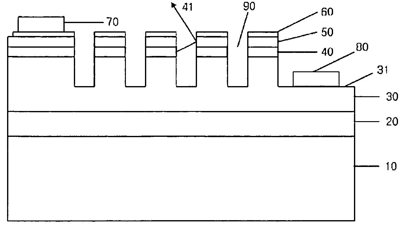
[0083]FIG. 9 is a plane view illustrating a semiconductor light emitting device in accordance with one embodiment of the present invention, and FIG. 10 is a schematic cross-sectional view taken along line A-B of FIG. 9. Here, the present invention is applied to a III-nitride semiconductor light emitting device. The light emitting device includes a substrate 10, a buffer layer 20 epitaxially grown on the substrate 10, an n-type nitride semiconductor layer 30 epitaxially grown on the buffer layer 20, an active layer 40 epitaxially grown on the n-type nitride semiconductor layer 30, a p-type nitride semiconductor layer 50 epitaxially grown on the active layer 40, a p-side electrode 60 formed on the p-type nitride semiconductor layer 50, a p-side bonding pad 70 formed on the p-side electrode 60, and an n-side electrod...


PUM


Abstract

The present invention discloses a semiconductor light emitting device including an active layer for generating light by recombination of electron and hole between a first semiconductor layer having first conductivity and a second semiconductor layer having second conductivity different from the first conductivity, the second semiconductor layer being disposed on the active layer. The semiconductor light emitting device comprises first array including a trench having a first inclination angle, and second array including a trench having a second inclination angle different from the first inclination angle.

Description

TECHNICAL FIELD[0001]The present invention relates to a semiconductor light emitting device, and more particularly, to a semiconductor light emitting device which can restrict inside heat generation and improve external quantum efficiency. The semiconductor light emitting device means a semiconductor device which emits light by using recombination of electron and hole, for example, a III-nitride semiconductor light emitting device.BACKGROUND ART[0002]FIGS. 1 and 2 are a cross-sectional view and a plane view illustrating one example of a conventional semiconductor light emitting device, namely, a III-nitride semi-conductor light emitting device. The conventional semiconductor light emitting device includes a substrate 1, a buffer layer 2 epitaxially grown on the substrate 1, an n-type nitride semiconductor layer 3 epitaxially grown on the buffer layer 2, an active layer 4 epitaxially grown on the n-type nitride semiconductor layer 3, a p-type nitride semi-conductor layer 5 epitaxiall...

Claims


Application Information

Patent Timeline
Patent Type & Authority Applications(United States)
IPC IPC(8): H01L33/00H01L33/08H01L33/20H01L33/38
CPCH01L33/38H01L33/20
Inventor YOO, TAE-KYUNGKIM, CHANG-TAEKIM, KEUK
Owner EPIVALLEY
Why Eureka
Try Eureka