Semiconductor light-emitting device and method for fabricating the same

a semiconductor and light-emitting device technology, applied in the direction of suction cups, mechanical equipment, fastening means, etc., can solve the problems of low external quantum efficiency of nitride compound semiconductors, low light extraction efficiency, etc., to reduce fabrication throughput and cost, high efficiency, and low cost

Inactive Publication Date: 2006-09-05
PANASONIC CORP
View PDF4 Cites 45 Cited by
  • Summary
  • Abstract
  • Description
  • Claims
  • Application Information

AI Technical Summary

Benefits of technology

[0010]It is therefore an object of the present invention to provide a light-emitting diode having a nitride compound semiconductor, which features high external quantum efficiency, stable characteristics, and easy design and processing.

Problems solved by technology

However, such a conventional structure has the problem of low light extraction efficiency.
The cause of the low light extraction efficiency is the refractivity of a semiconductor which is higher than that of the air.
Thus, the conventional LED using a nitride compound semiconductor is low in external quantum efficiency (the ratio of light that can be extracted from the LED to currents supplied to the LED) and has the problem of power conversion efficiency (the ratio of a light output that can be produced to all the supplied power) lower than that of a fluorescent lamp.
However, the technology for improving the light extraction efficiency based on the principle proposed in Prior Art Document 1 is disadvantageous in that, because the angle of incidence of light sensitively varies in response to the configuration of a projecting and depressed surface, the design of the projecting and depressed surface is extremely difficult and characteristics are unstable due to size variations during the fabrication of devices.
The technology is also disadvantageous in that, though the projections / depressions to be formed should have a depth of about several micrometers to improve the light extraction efficiency, processing is difficult because of the high etching resistance of a nitride compound semiconductor.

Method used


Image

  • Semiconductor light-emitting device and method for fabricating the same
  • Semiconductor light-emitting device and method for fabricating the same
  • Semiconductor light-emitting device and method for fabricating the same

Examples


embodiment 1

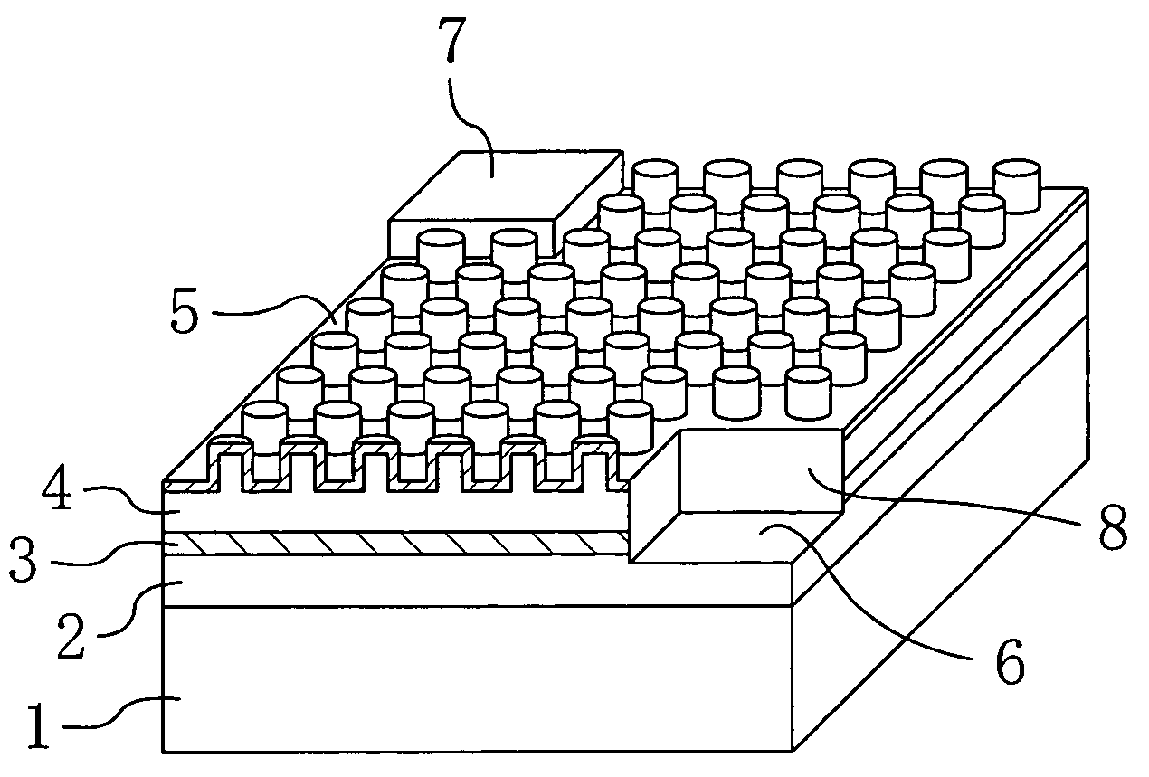
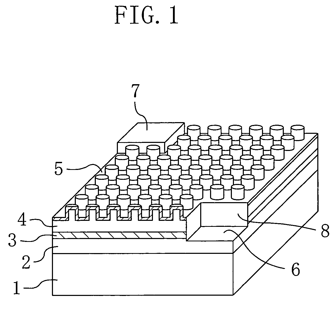
[0048]FIG. 1 is a perspective view showing a structure of a semiconductor light-emitting device according to a first embodiment of the present invention. As shown in FIG. 1, the semiconductor light-emitting device according to the present embodiment is an LED comprising: a sapphire substrate 1; a non-doped GaN buffer layer (not shown) provided on the sapphire substrate 1 and having a thickness of 30 nm; an n-type GaN layer 2 provided on the GaN buffer layer, doped with an n-type impurity at a concentration of 2×1018 cm−3, and having a thickness of 2 μm; an InGaN active layer 3 provided on the n-type GaN layer 2, made of non-doped In0.45Ga0.55N with a PL (photoluminescence) peak wavelength of 450 nm, and having a thickness of 3 nm; and a p-type GaN layer 4 doped with a p-type impurity at a concentration of 7×1017 cm−3 and having a thickness of 400 nm. These nitride compound semiconductors are formed by crystal growth such as MOCVD (Metal-Organic Chemical Vapor Deposition) or MBE (Mol...

embodiment 2

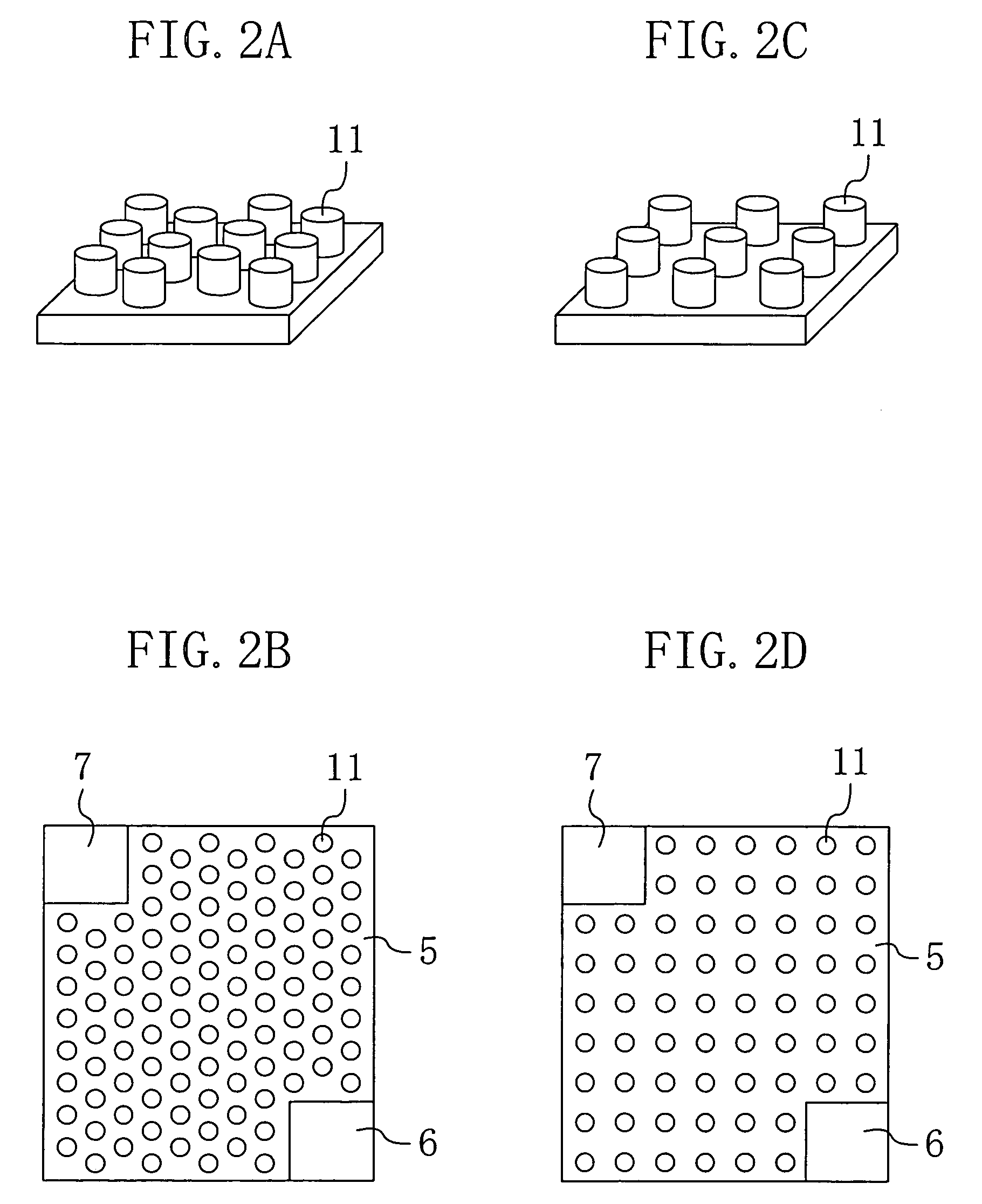
[0066]FIG. 13 is a perspective view showing a structure of a semiconductor light-emitting device according to a second embodiment of the present invention. As shown in FIG. 13, the semiconductor light-emitting device according to the present embodiment is an LED comprising: a sapphire substrate 1; a non-doped GaN buffer layer (not shown) provided on the sapphire substrate 1 and having a thickness of 30 nm; an n-type GaN layer 2 provided on the GaN buffer layer, doped with an n-type impurity at a concentration of 2×1018 cm−3, and having a thickness of 2 μm; an InGaN active layer 3 provided on the n-type GaN layer 2, made of non-doped In0.45Ga0.55N with a PL peak wavelength of 450 nm, and having a thickness of 3 nm; and a p-type GaN layer 4 provided on the InGaN active layer 3, doped with a p-type impurity at a concentration of 7×1017 cm−3, and having a thickness of 200 nm.

[0067]A trench 8 for exposing the n-type GaN layer as the upper surface thereof has been formed by partly etching...

embodiment 3

[0072]FIG. 14 is a perspective view showing a structure of a semiconductor light-emitting device according to a third embodiment of the present invention. As shown in FIG. 14, the semiconductor light-emitting device according to the present embodiment is an LED comprising: a sapphire substrate 1; a non-doped GaN buffer layer (not shown) provided on the sapphire substrate 1 and having a thickness of 30 nm; an n-type GaN layer 2 provided on the GaN buffer layer, doped with an n-type impurity at a concentration of 2×1018 cm−3, and having a thickness of 2 μm; an InGaN active layer 3 provided on the n-type GaN layer 2, made of non-doped In0.45Ga0.55N at a PL peak wavelength of 450 nm, and having a thickness of 3 nm; and a p-type GaN layer 4 provided on the InGaN active layer 3, doped with a p-type impurity at a concentration of 7×1017 cm−3, and having a thickness of 200 nm. These nitride compound semiconductors are formed by crystal growth such as MOCVD or MBE.

[0073]A trench 8 for exposi...


PUM


Abstract

Projections / depressions of a two-dimensional periodic structure are formed in a p-GaN layer (4) such that the period of the projections / depressions is 1 to 20 times the wavelength of light radiated from an active layer (3) in a semiconductor. As a result, a diffractive effect achieved by the projections / depressions of the two-dimensional periodic structure change the direction in which the light radiated from the active layer (3) travels. If the projections / depressions are not provided, light at a radiation angle which satisfies conditions for total reflection at the interface between a semiconductor device and an air cannot be extracted to the outside of the semiconductor device so that the light emission efficiency of the device is low. By contrast, the projections / depressions as formed with a period according to the present invention diffract the light at an angle which does not cause total reflection so that the efficiency with which the light is extracted to the outside of the semiconductor device is improved exponentially. This improves the light emission efficiency of the device.

Description

BACKGROUND OF THE INVENTION[0001]The present invention relates to a semiconductor light-emitting device and, more particularly, to a semiconductor light-emitting device made of a nitride compound semiconductor such as GaN, InGaN, AlGaN, or the like.[0002]In recent years, the use of a nitride compound semiconductor represented by GaN has allowed a high-intensity emission of light ranging in color from ultraviolet to blue and green, which had been impossible thus far. As a result, light-emitting devices using nitride compound semiconductors, such as a light-emitting diode (LED) and a semiconductor laser, have been developed vigorously. Since an LED is easier to fabricate and control than a semiconductor laser and longer in lifespan than a fluorescent lamp, an LED using a nitride compound semiconductor is considered to be promising as a light source for illumination.[0003]A description will be given herein below to an example of a conventional nitride compound semiconductor LED. FIG. 1...

Claims


Application Information

Patent Timeline
Patent Type & Authority Patents(United States)
IPC IPC(8): H01L33/00H01L33/20H01L33/38H01L33/42
CPCH01L33/20H01L2933/0083H01L33/42H01L33/38E03C1/06F16B47/00
Inventor ORITA, KENJI
Owner PANASONIC CORP
Why Eureka
Try Eureka