Organic electroluminescent device

a technology of electroluminescent devices and organic materials, applied in the direction of discharge tubes/lamp details, discharge tubes luminescent screens, organic semiconductor devices, etc., can solve the problem of limited light in the device, and achieve the effect of increasing external quantum efficiency and luminescent efficiency

Active Publication Date: 2005-04-28
IND TECH RES INST
View PDF5 Cites 45 Cited by
  • Summary
  • Abstract
  • Description
  • Claims
  • Application Information

AI Technical Summary

Benefits of technology

[0007] Accordingly, an object of the present invention is to provide an OLED comprising a nanostructured organic electroluminescent recovery layer, with dielectric material and nanoscale metal particles. The surface plasmon resonance of OLED device is cross-coupled to the surface plasmon resonance of nanostructured film. Trapped device light is thus recovered, increasing external quantum efficiency and luminescent efficiency.

Problems solved by technology

In addition, the organic material and the glass substrate have a higher refraction index than air, so some light is limited in the device due to total reflection, some scattering outward from the device side.

Method used


Image

  • Organic electroluminescent device
  • Organic electroluminescent device
  • Organic electroluminescent device

Examples


first embodiment

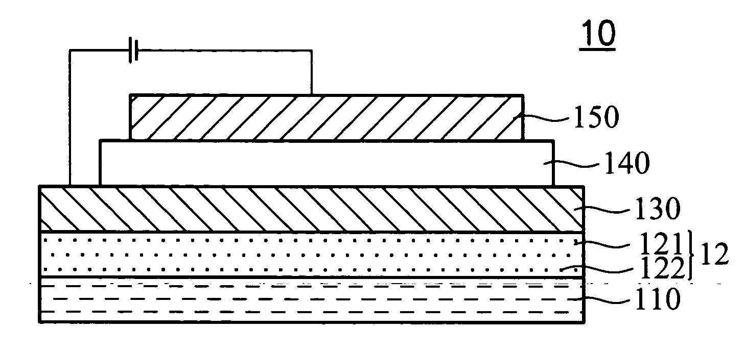
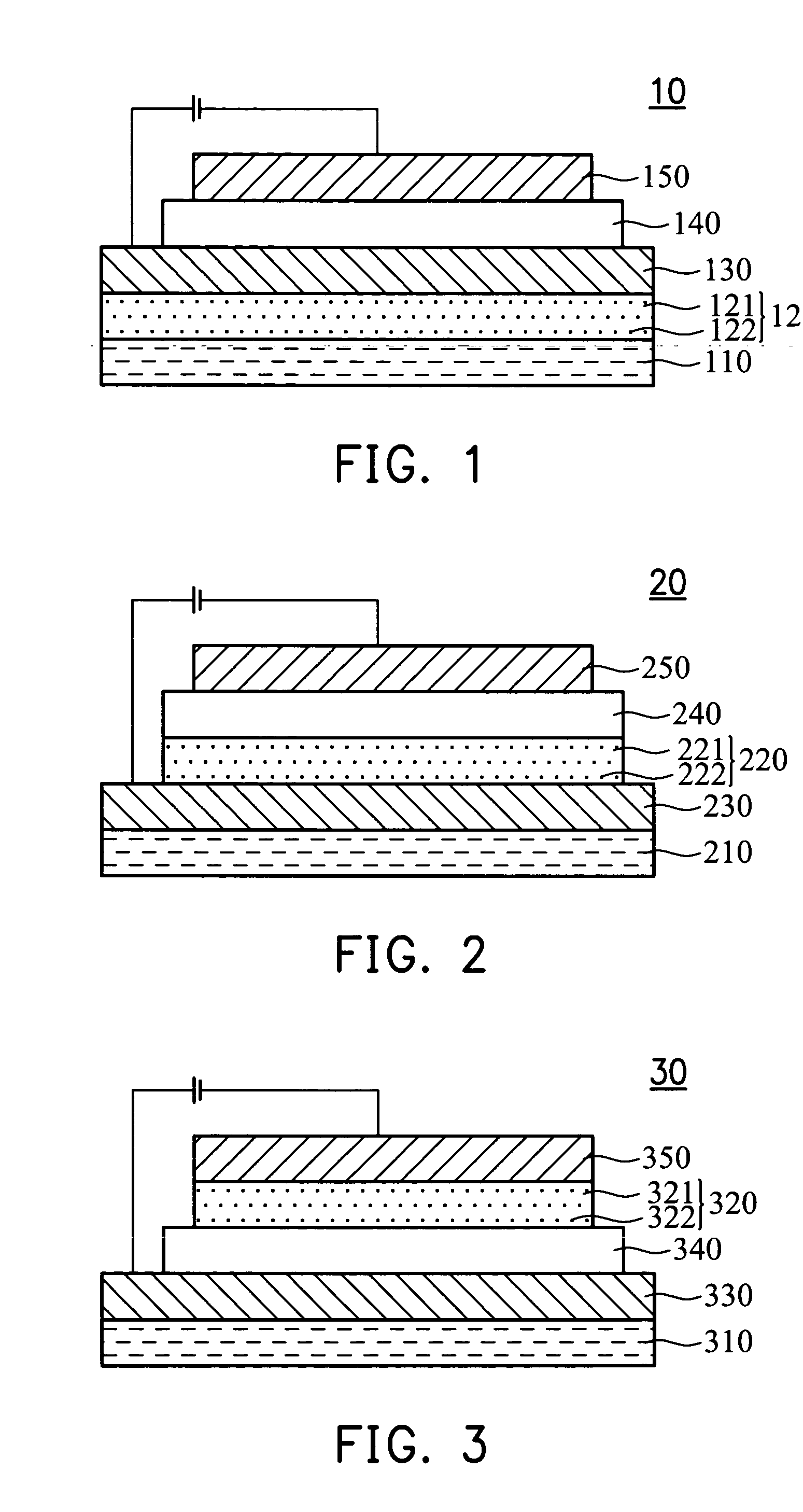
[0036] First, a substrate 110 is provided as FIG. 1, transparent or opaque, formed with glass or plastic (flexible) material.

[0037] Nanostructured organic electroluminescent recovery layer 120 is formed with dielectric or organic material 121 and nanoscale metal particles 122 on the substrate 121. The dielectric or organic material 121 and the nanoscale metal particles 122 are formed at the same time using the same or different methods. The nanoscale metal particles 122 are doped into the dielectric or organic material 121. The dielectric material for the nanostructured organic electroluminescent recovery layer is silicon oxide, aluminum oxide, magnesium oxide, silicon nitride, aluminum nitride or magnesium fluoride, and is formed by sputtering or plasmon enhanced chemical vapor deposition. The organic material for the nanostructured organic electroluminescent recovery layer is molecular or polymer organic material, formed by thermal evaporation, spin coating, ink jet, or screen pr...

second embodiment

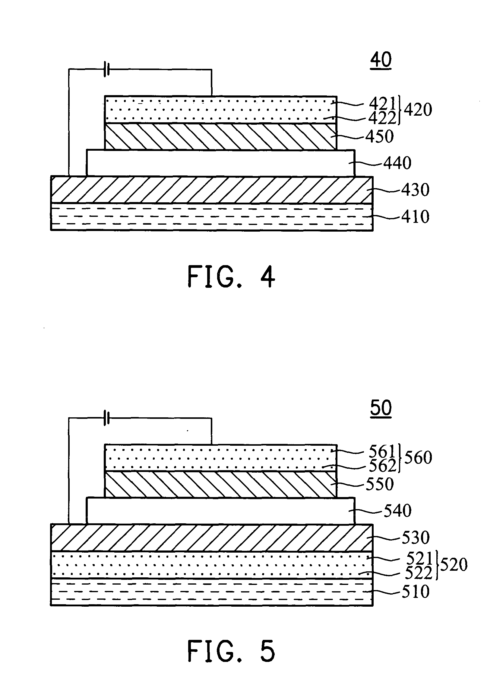
[0042] The nanostructured organic electroluminescent recovery layer 220 of this embodiment differs only from the previous embodiment in that the nanostructured organic electroluminescent recovery layer 220 is between the first electrode 230 and the organic luminescent layer 240.

third embodiment

[0043] The nanostructured organic electroluminescent recovery layer 320 of this embodiment differs only from the previous embodiments in that the nanostructured organic electroluminescent recovery layer 320 is between the organic luminescent layer 340 and the second electrode 350.


PUM


Abstract

An organic electroluminescent device. The device has an organic electroluminescent light recovery layer consisting of dielectric material and nanoscale metal particles or organic material and nanoscale metal particles. The membrane of the organic electroluminescent light recovery layer cross couples with surface plasmon resonance and recovers light trapped in the device, enhancing the light emission efficiency of the organic electroluminescent device.

Description

BACKGROUND OF THE INVENTION [0001] 1. Field of the Invention [0002] The present invention relates to an organic electroluminescent device, and more particularly to an organic electroluminescent device solving low external quantum efficiency problems of surface plasmon resonance. [0003] 2. Description of the Related Art [0004] Organic electroluminescent devices are also known as organic light emitting diodes (OLED). The OLED luminescent principle applies a voltage to organic molecular material or polymer material, and the device luminesces. Due to OLED's self emission characteristics, it can form a dot matrix type display with light weight, slim profile, high contrast, low power consumption, high resolution, fast response time, no need for backlighting, and full viewing angle. Possible display parameters range from 4 mm microdisplay to 100 inch outdoor billboards, making it a preferred type of flat panel display (FPD). If the OLED luminescent efficiency is over 100 Lm / W, it can repla...

Claims


Application Information

Patent Timeline
Patent Type & Authority Applications(United States)
IPC IPC(8): H01J1/62H01J63/04H05B33/02H01L51/50H01L51/52H05B33/14H05B33/22
CPCB82Y20/00H01L2251/5369H01L51/5262B82Y30/00H10K2102/331H10K50/852H10K50/85
Inventor TSENG, MEI-RURNGLIU, JONG-MINWANG, JUEN-KAILIN, HSIEN-KUANG
Owner IND TECH RES INST
Why Eureka
Try Eureka