Transflective liquid crystal display device and fabrication method thereof

a liquid crystal display device and transflective technology, applied in non-linear optics, instruments, optics, etc., can solve the problems of inability to achieve maximum light efficiency in both transmissive and reflective modes of transflective lcds, difficulty in conserving weight, volume, power consumption of transmissive lcds, etc., to achieve maximum light efficiency and ameliorate the disadvantages of conventional technology

Active Publication Date: 2005-01-06
HANNSTAR DISPLAY CORPORATION
View PDF1 Cites 94 Cited by
  • Summary
  • Abstract
  • Description
  • Claims
  • Application Information

AI Technical Summary

Benefits of technology

[0015] The present invention improves on the conventional technology in that the first orientation control window having a slit width “Src” is formed between the first common electrodes in an area corresponding to each first pixel electrode. The second orientation control window having a slit width “Stc” is formed between the second common electrodes in an area corresponding to each second pixel electrode. Specially, a relationship between “Src” and “Stc” satisfies Src<Stc. According to the present invention, the effective birefringence (Δneff) in the reflective region can be different from that in the transmissive region, thereby achieving maximum light efficiency in both reflective and transmissive modes under saturation voltage and ameliorating the disadvantages of the conventional technology.

Problems solved by technology

It is difficult to conserve weight, volume, and power consumption of transmissive LCDs due to the power requirements of the backlight component.
The conventional structure of slits between electrodes, nevertheless, is not presently applied to the transflective LCD device.
That is, the conventional configuration cannot achieve maximum light efficiency in both transmissive and reflective modes in the transflective LCD device.

Method used


Image

  • Transflective liquid crystal display device and fabrication method thereof
  • Transflective liquid crystal display device and fabrication method thereof
  • Transflective liquid crystal display device and fabrication method thereof

Examples


Embodiment Construction

[0023] Reference will now be made in detail to the present preferred embodiments of the invention, examples of which are illustrated in the accompanying drawings. Wherever possible, the same reference numbers are used in the drawings and the description to refer to the same or like parts.

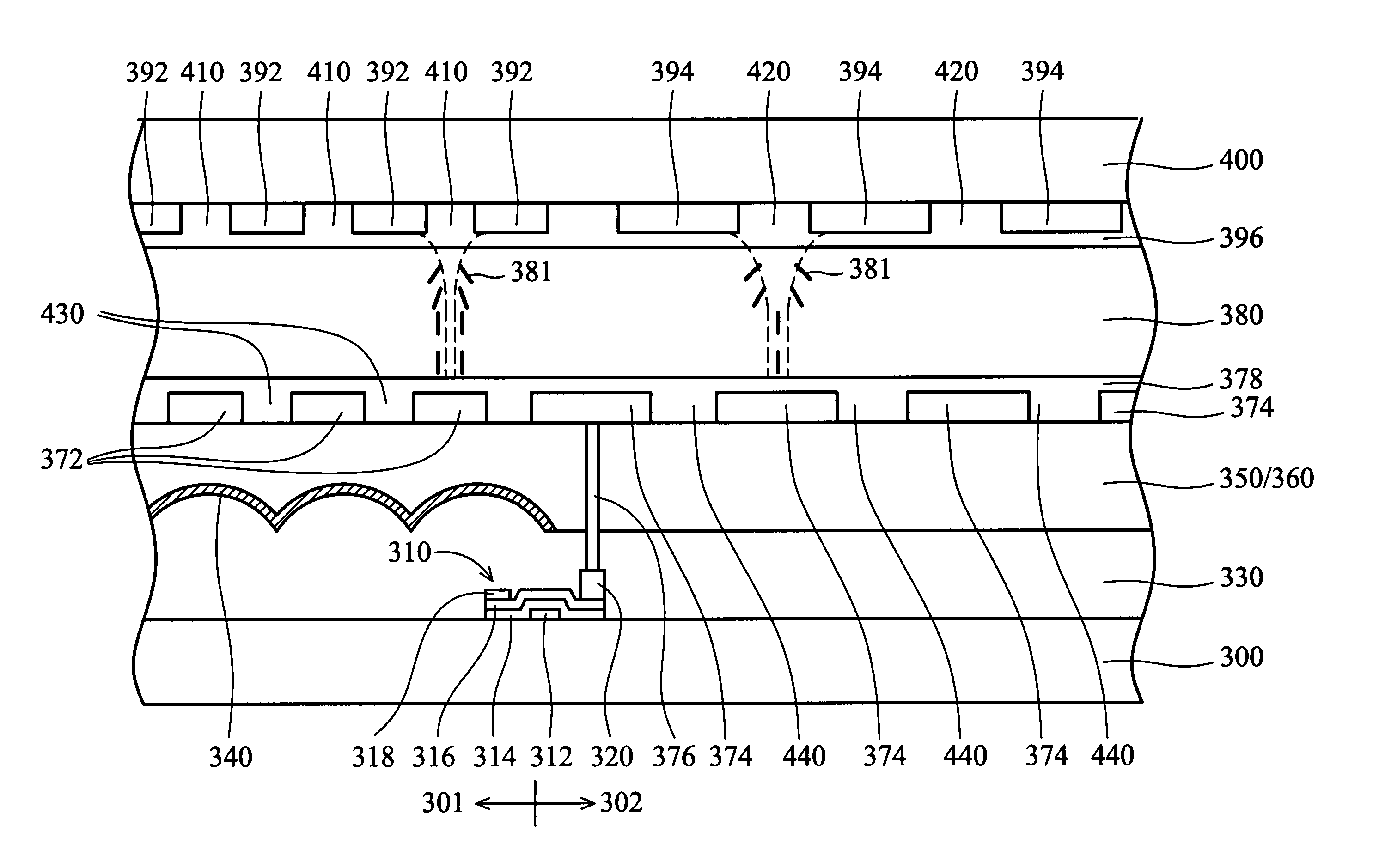
[0024]FIG. 3 is a sectional view of a transflective LCD device with a single cell gap according to the present invention. In order to simplify the illustration, FIG. 3 shows a substrate in a single pixel region, although pixel regions may be numerous.

[0025] A first substrate 300 serving as a lower substrate comprises a predetermined reflective region (or section) 301 and a predetermined transmissive region (or section) 302. The first substrate 300 may be a heat-resistant glass substrate.

[0026] A pixel driving device array overlies the first substrate 300. The pixel driving device array may be a thin film transistor (TFT) 310 array. The TFT device 310 comprises a gate 312, a gate insulating layer ...


PUM

PropertyMeasurementUnit
slit widthaaaaaaaaaa
widthaaaaaaaaaa

Abstract

A transflective LCD device with a single cell gap. First and second pixel electrodes are formed on the lower substrate. First and second common electrodes are formed on an inner surface of the upper substrate. The first pixel electrodes and the first common electrodes are located in the reflective region. The second pixel electrodes and the second common electrodes are located in the transmissive region. A first orientation control window having a slit width “Src” is formed between the first common electrodes in an area corresponding to each first pixel electrode. A second orientation control window having a slit width “Stc” is formed between the second common electrodes, satisfying Src<Stc. The second orientation control window is in an area corresponding to each second pixel electrode. Accordingly, maximum light efficiency can be achieved in both reflective and transmissive modes.

Description

BACKGROUND OF THE INVENTION [0001] 1. Field of the Invention [0002] The present invention relates to a vertically aligned (VA) transflective liquid crystal display device, and more particularly, to a VA transflective liquid crystal display device with a single cell gap. [0003] 2. Description of the Related Art [0004] Liquid crystal display (LCD) devices are widely used for portable televisions, notebook computers and other applications. Liquid crystal display devices are classified into transmissive devices using a backlight as a light source, and reflective devices using an external light source, such as sunlight or indoor lamp. It is difficult to conserve weight, volume, and power consumption of transmissive LCDs due to the power requirements of the backlight component. Reflective LCDs have the advantage of no backlight component, but cannot operate without an external light source. [0005] An alternative to these types of LCDs is a transflective LCD device which can operate both r...

Claims


Application Information

Patent Timeline
Patent Type & Authority Applications(United States)
IPC IPC(8): G02F1/1333G02F1/1335G02F1/1337G02F1/1343G02F1/1368G02F1/139
CPCG02F1/133555G02F2001/134318G02F1/1393G02F1/133707G02F1/134318
Inventor CHANG, CHING CHAO
Owner HANNSTAR DISPLAY CORPORATION
Why Eureka
Try Eureka