
Plane emission device
a technology of emission device and emission chamber, which is applied in the direction of discharge tube luminescnet screen, semiconductor/solid-state device details, transportation and packaging, etc., can solve the problems of reducing the luminous efficiency of the organic el device, and achieve the effect of increasing the incident efficiency of lights to the transparent substrate and increasing the takeout efficiency of lights to the outsid
- Summary
- Abstract
- Description
- Claims
- Application Information
AI Technical Summary
Benefits of technology
Problems solved by technology
Method used
Image

Examples
first embodiment
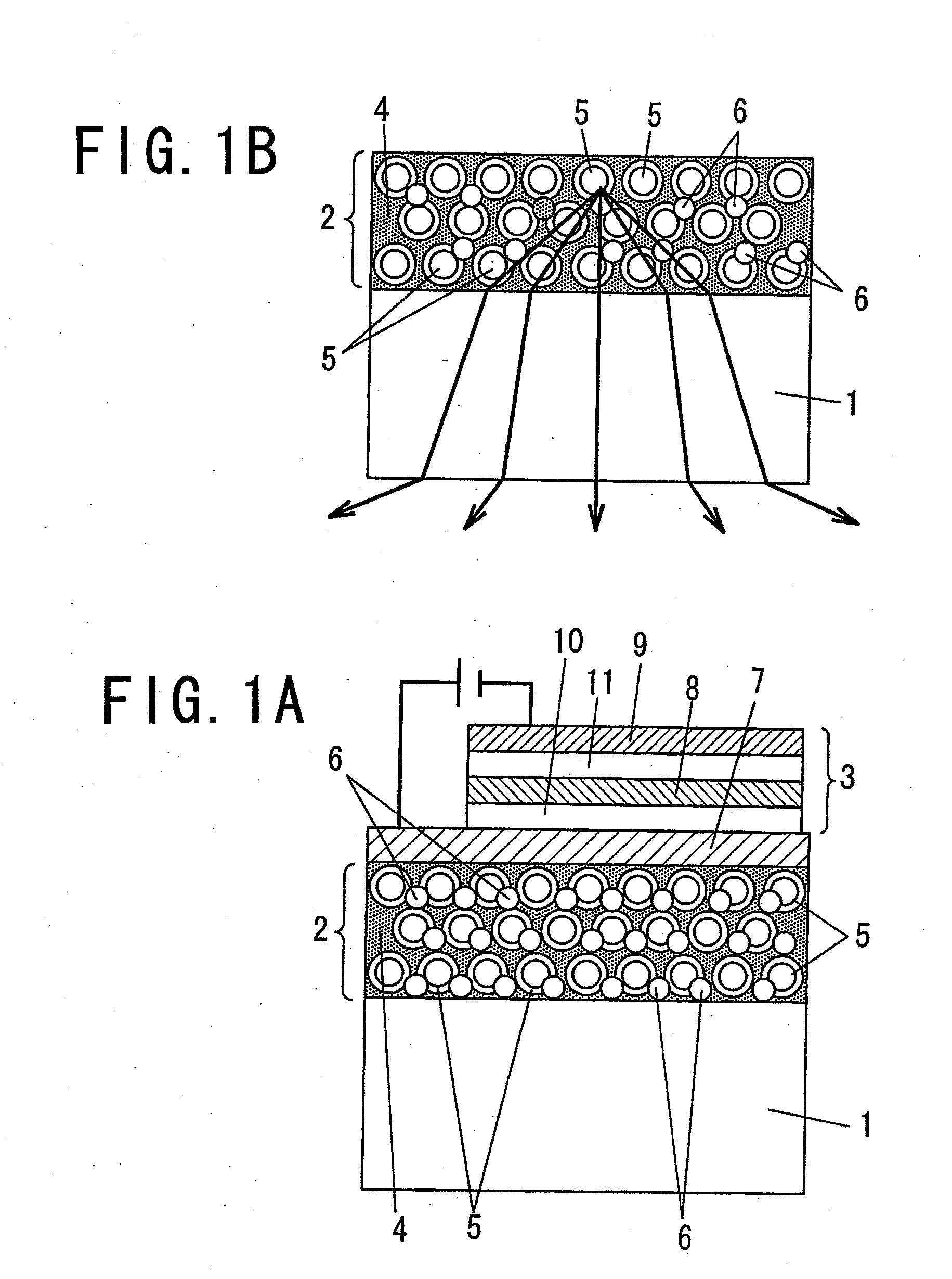
[0017]A plane emission device in accordance with a first embodiment of the present invention is described with reference to FIG. 1A and FIG. 1B. FIG. 1A shows a configuration of a plane emission device in accordance with the first embodiment, and FIG. 1B shows a configuration of a light scattering layer 2 formed on a surface of a transparent substrate 1.
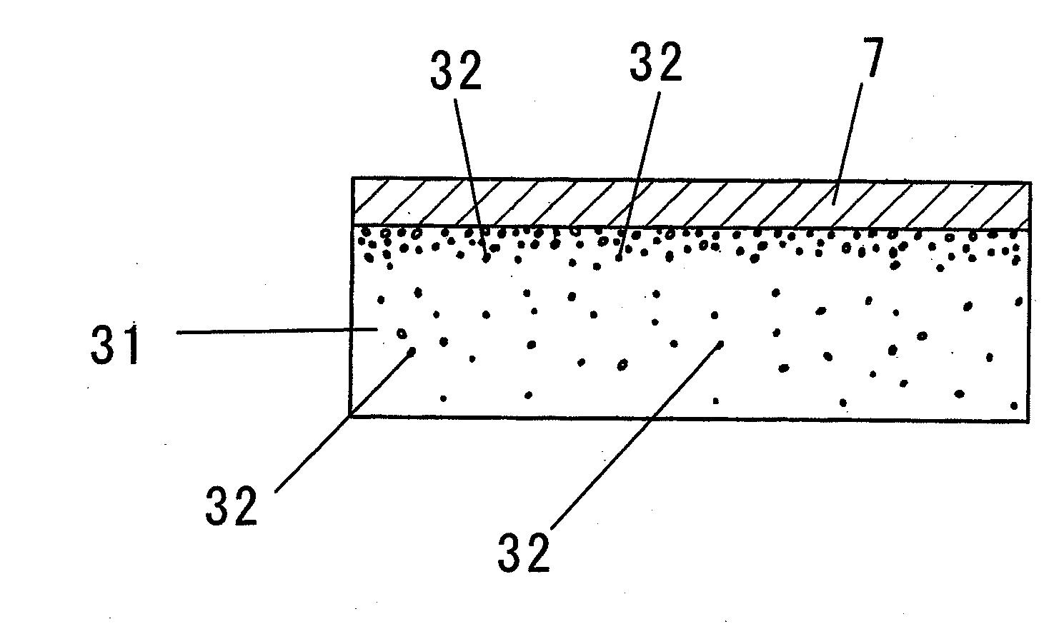
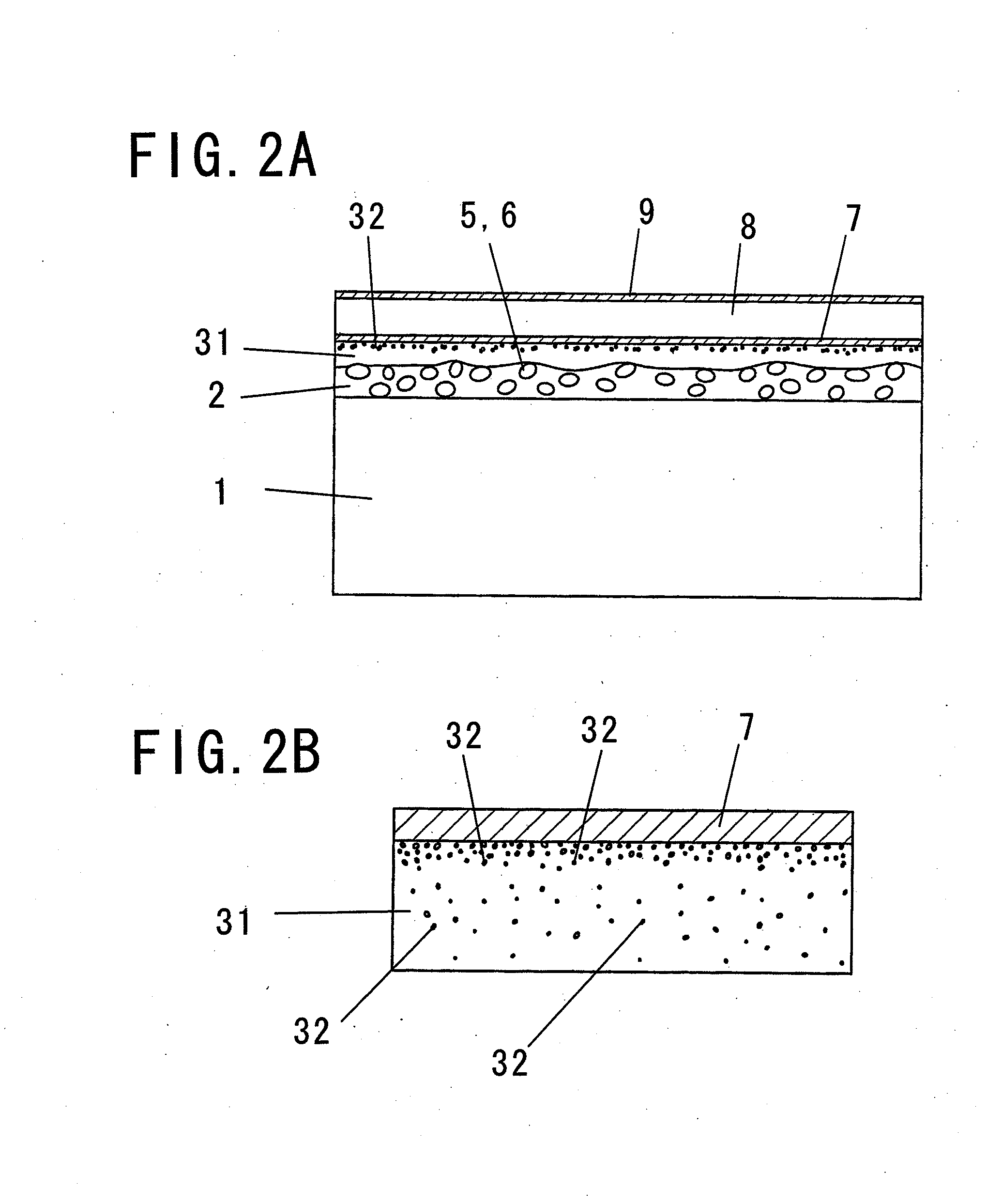
[0018]As for a luminescent body 3, an organic or an inorganic one which emits lights by light or electric energy can be used. The luminescent body 3 shown in FIG. 1A is one which emits lights owing to be activated by electric energy, such as an organic EL device. The luminescent body 3 is configured of a transparent electrode layer (anode) 7 which is formed on the light scattering layer 2, a luminescent layer 8, an opposing electrode (cathode) 9 and a hole transfer layer 10 and an electron transfer layer 11 which are provided according to need, and so on. Lights emitted in the luminescent layer 8 pass through the transparent electrod...
example 1
Practical Example 1
[0042]A solution was obtained by adding 803.5 masses part of isopropyl alcohol into 86.8 masses part of tetraethoxysilane, and further adding 34.7 mass part of γ-methacryloxypropyltrymethoxysilane and 75 mass part of 0.1N-nitric acid, and mixing it well with by dispersion mill. The obtained solution was agitated two hours in thermostatic oven at 40 degrees Celsius, and thus, 5 weight % of silicone resin solution was obtained as a binder silicone resin having 1050 weight average molecular weight.
[0043]Subsequently, a silicone resin solution containing hollow silica fine particles was obtained by adding a sol that an IPA dispersed sol (solid content: 20 mass %, dispersion medium: isopropyl alcohol, made by Catalysts and Chemicals Ltd.) of hollow silica fine particles (mean particle diameter: 60 nm, outer shell thickness: 10 nm) was diluted by isopropyl alcohol to be 5 mass % into the silicone resin solution so that hollow silica fine particles / silicone resin (conden...
example 2
Practical Example 2
[0052]In order to make the refraction index of the light scattering layer 2 smaller than the refraction index of the transparent substrate 1, a coating materials composition was prepared by adding hollow silica fine particles / silica-titania compound fine particles / silicone resin (condensation chemical compound conversion) into silicone resin solution obtained in the above mentioned practical example 1 so as to be 60 / 10 / 30 on the basis of solid content mass standard, and a light scattering layer 2 was formed with this coating materials composition similar to the practical example 1. The refraction index of the light scattering layer 2 was 1.39 which was smaller than the refraction index 1.51 of the transparent substrate 1. Then, an organic EL device (luminescent body) 3 was formed on the light scattering layer 2 similar to the practical example 1, and thus, a plane emission device was obtained.
PUM
| Property | Measurement | Unit |
|---|---|---|
| mean particle diameters | aaaaa | aaaaa |
| diameter | aaaaa | aaaaa |
| transparent | aaaaa | aaaaa |
Abstract
Description
Claims
Application Information