Semiconductor device and method of manufacturing the same

a technology of semiconductors and semiconductors, applied in the direction of semiconductor devices, basic electric elements, electrical equipment, etc., can solve the problems of difficult to suppress the deterioration of morphology

Active Publication Date: 2005-01-13
KIOXIA CORP
View PDF3 Cites 30 Cited by
  • Summary
  • Abstract
  • Description
  • Claims
  • Application Information

AI Technical Summary

Benefits of technology

[0043]FIG. 4 is a cross sectional view schematically sh

Problems solved by technology

However, in the case of forming a silicide film on the SiGe film,

Method used


Image

  • Semiconductor device and method of manufacturing the same
  • Semiconductor device and method of manufacturing the same
  • Semiconductor device and method of manufacturing the same

Examples


Embodiment Construction

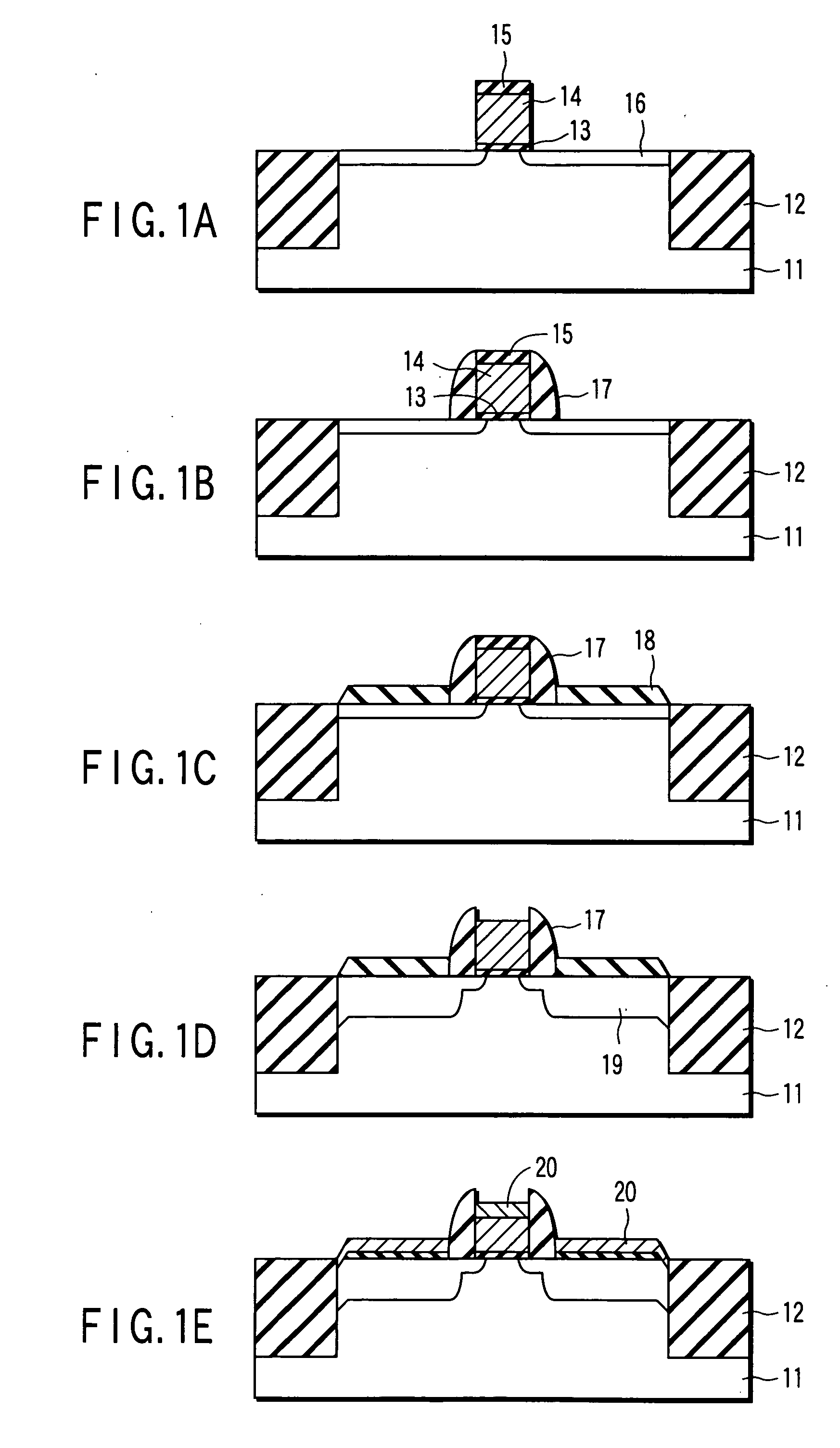
[0049] As a result of an extensive research on the combination of a so-called “SiGe elevated source-drain technology”, in which the source-drain layers are elevated at a low temperature by forming a SiGe film by a selective epitaxial growth, and the salicide technology, the present inventors have found the situation described in the following.

[0050] First of all, it has been found that the following problem is generated if the silicon epitaxial growth technology is simply replaced by the SiGe technology in the elevated source-drain process.

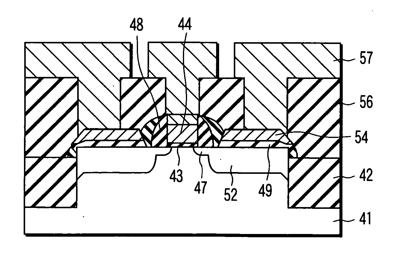
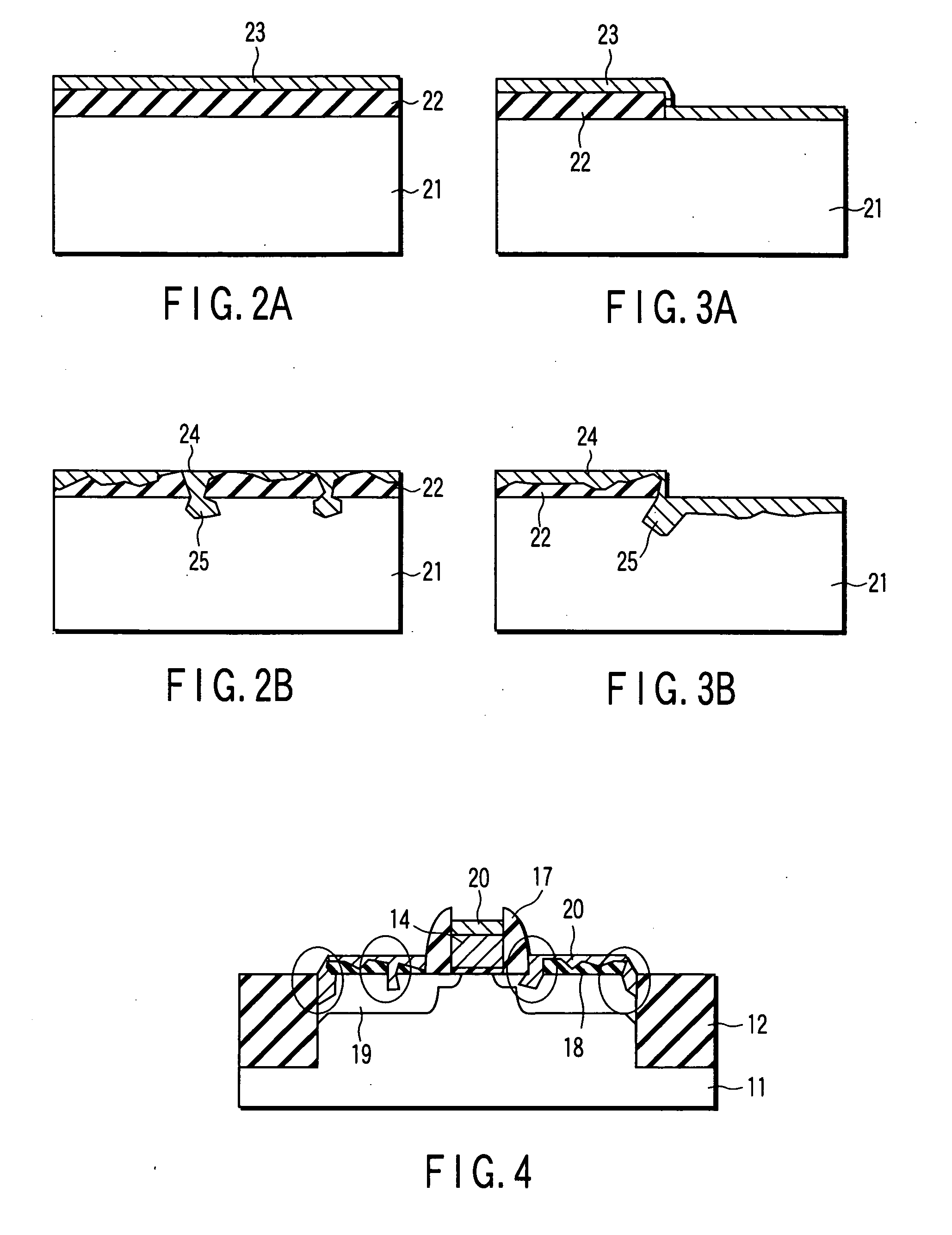
[0051] Specifically, where a NiSi film is formed on a thin SiGe film, a SiGe film 22 and a Ni film 23 are formed successively on a silicon substrate 21 as shown in FIG. 2A, followed by applying a heat treatment. It should be noted that the interface between a NiSi film 24 and the SiGe film 22 cannot be made completely flat because of the influence of, for example, the grain boundary. In other words, the interface noted above is rendered irregula...


PUM


Abstract

There is disclosed is a semiconductor device which comprises a semiconductor substrate, isolation regions formed within the semiconductor substrate to define the active region, a pair of impurity diffusion regions formed within the element region in a manner to have surfaces elevated from the isolation region, a SiGe film formed on an upper surface of the impurity diffusion region so as to cover partly the side surface of the impurity diffusion region, a Ge concentration in the SiGe film being higher at a lower surface of the SiGe film than at an upper surface of the SiGe film, a metal silicide layer formed on the SiGe film, and a gate electrode formed in the active region of the semiconductor substrate with a gate insulating film interposed therebetween and having a sidewall insulating film formed on the side surface.

Description

CROSS-REFERENCE TO RELATED APPLICATIONS [0001] This application is based upon and claims the benefit of priority from the prior Japanese Patent Application No. 2003-273603, filed Jul. 11, 2003, the entire contents of which are incorporated herein by reference. BACKGROUND OF THE INVENTION [0002] 1. Field of the Invention [0003] The present invention relates to a semiconductor device, particularly, to a MIS (Metal Insulator Semiconductor) type FET (Field Effect Transistor) having a silicide film in an upper portion of the source-drain diffusion layers. [0004] 2. Description of the Related Art [0005] In recent years, an elevated source-drain technology is proposed in order to suppress the problem in respect of a junction leak defect of a transistor. [0006] The MOS type FET device having an elevated source-drain structure is manufactured by the process shown in, for example, FIGS. 1A to 1E. [0007] In the first step, an isolation region 12 consisting of a silicon oxide film is formed in ...

Claims


Application Information

Patent Timeline
IPC IPC(8): H01L21/336H01L21/28H01L29/165H01L29/417H01L29/423H01L29/49H01L29/78
CPCH01L29/165H01L29/66477H01L29/66628H01L29/66545H01L29/6656H01L29/665
Inventor IINUMA, TOSHIHIKOMIZUSHIMA, ICHIROIZUHA, MITSUAKIMIYANO, KIYOTAKASUGURO, KYOICHI
Owner KIOXIA CORP
Why Eureka
Try Eureka