Nonvolatile memory devices and methods of forming the same

a non-volatile memory and memory device technology, applied in semiconductor devices, solid-state devices, instruments, etc., can solve the problems of avoiding over-erase effects, and reducing the size of non-volatile memory devices

Inactive Publication Date: 2006-04-06
SAMSUNG ELECTRONICS CO LTD
View PDF13 Cites 26 Cited by
  • Summary
  • Abstract
  • Description
  • Claims
  • Application Information

AI Technical Summary

Problems solved by technology

Volatile memory loses any stored data as soon as the system is turned off.
It is known that stacked gate cells suffer from over-erase effects.
The over-erase effects occur when a floating gate is excessively discharged during an erasing operation at a stacked gate memory cell.
However, in the case of such a two-transistor memory c...

Method used


Image

  • Nonvolatile memory devices and methods of forming the same
  • Nonvolatile memory devices and methods of forming the same
  • Nonvolatile memory devices and methods of forming the same

Examples


Embodiment Construction

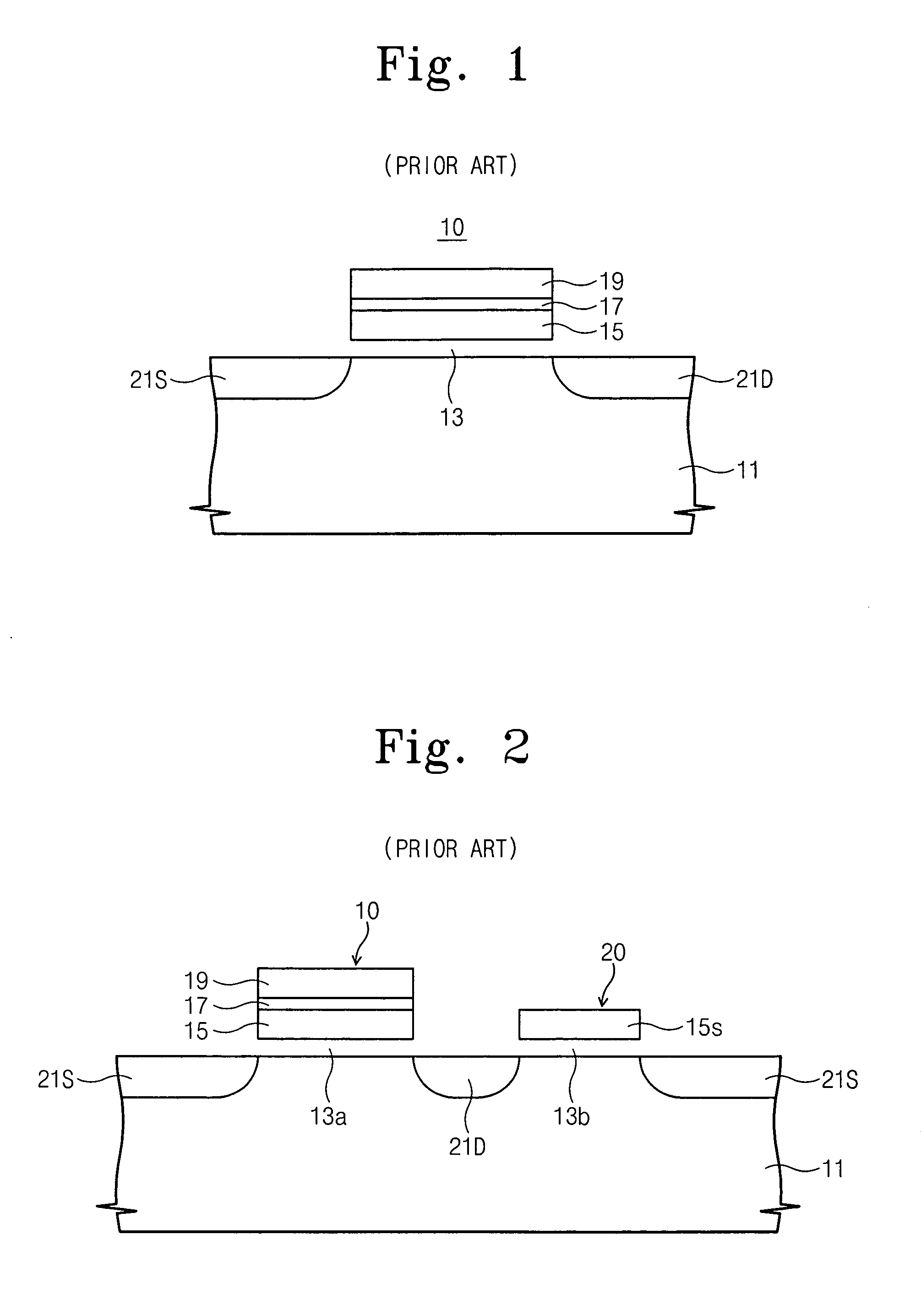
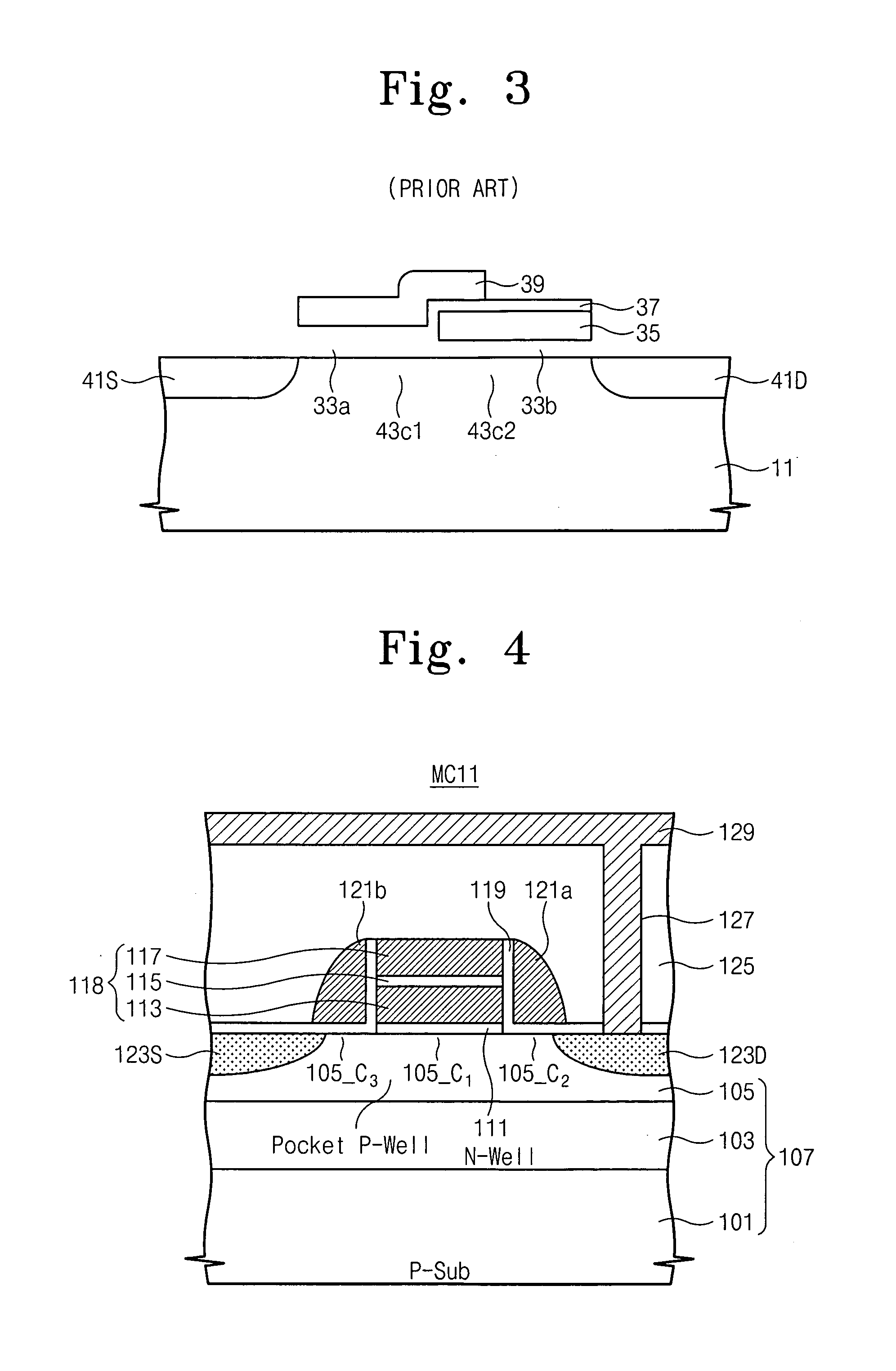
[0038] The present invention will now be described more fully hereinafter with reference to the accompanying drawings, in which preferred embodiments of the invention are shown. The invention may, however, be embodied in different forms and should not be construed as limited to the embodiments set forth herein. Rather, these embodiments are provided so that this-disclosure will be thorough and complete, and will fully convey the scope of the invention to those skilled in the art. In the drawings, the height of layers and regions are exaggerated for clarity. It will also be understood that when a layer is referred to as being “on” another layer or substrate, it can be directly on the other layer or substrate, or intervening layers may also be present. Like numbers refer to like elements throughout the description of the figures.

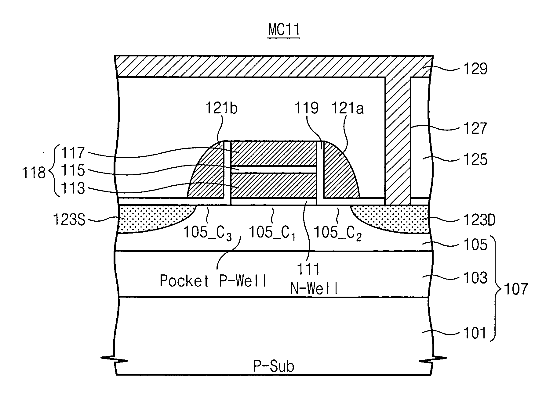
[0039]FIG. 4 and FIG. 5 are cross-sectional views of a unit nonvolatile memory cell according to an embodiment of the present invention. Specifically, FIG. 4...


PUM


Abstract

A nonvolatile memory device includes first and second impurity diffusion regions formed in a semiconductor substrate, and a memory cell formed on a channel region of a semiconductor substrate between the first and second impurity diffusion regions. The memory cell includes a stacked gate structure formed on the channel region, and first and second select gates formed on the channel regions and opposite sidewalls of the stacked gate structure. Since the first and second select gates are spacer-shaped to be self-aligned on opposite sidewalls of the stacked gate structure, a size of a memory cell is reduced to enhance an integration density of a semiconductor device.

Description

BACKGROUND OF THE INVENTION [0001] 1. Field of the Invention [0002] The present invention relates to semiconductor devices and methods of forming the same. More specifically, the present invention is directed to nonvolatile memory devices and methods of forming the same. [0003] 2. Description of the Related Art [0004] Memory can be split into two main categories: volatile and nonvolatile. Volatile memory loses any stored data as soon as the system is turned off. Electrically erasable programmable read-only memories (EEPROMs) are a kind of nonvolatile memory which keep stored data even when their power supplies are interrupted. [0005] Generally, memory cell structures of nonvolatile memory devices may be classified into two categories, namely, a split gate structure and a stacked gate structure. A conventional stacked gate memory cell is illustrated in FIG. 1. As shown in FIG. 1, a floating gate 15 and a control gate 19 are sequentially stacked on a substrate 11. A tunneling oxide la...

Claims


Application Information

Patent Timeline
IPC IPC(8): H01L21/8238H01L29/788
CPCG11C16/0433H01L27/115H01L27/11521H01L29/42328H01L29/7885H10B69/00H10B41/30H01L21/823468
Inventor KOH, KWANG-WOOKHAN, JEONG-UK
Owner SAMSUNG ELECTRONICS CO LTD
Why Eureka
Try Eureka