Semiconductor device and manufacturing method thereof

a semiconductor and semiconductor technology, applied in the direction of semiconductor devices, electrical appliances, transistors, etc., can solve the problems of difficult control of threshold voltage, difficult to reduce threshold voltage, problematically reduce etc., to reduce the threshold voltage of transistors, facilitate threshold voltage control, and suppress transistor fluctuations.

Inactive Publication Date: 2009-12-24
ELPIDA MEMORY INC
View PDF24 Cites 29 Cited by
  • Summary
  • Abstract
  • Description
  • Claims
  • Application Information

AI Technical Summary

Benefits of technology

[0040]Therefore, a reduction in the threshold voltage of a transistor due to a short channel effect is prevented to facilitate threshold voltage control.
[0041]In addition, fluctuations in the threshold voltage of the transistor can be suppressed.

Problems solved by technology

As a result, the threshold voltage of the transistor is problematically reduced.
Therefore, when the gate length is reduced as semiconductor device miniaturization progresses, there is a problem that the threshold voltage of the transistor decreases due to a short channel effect, thereby making it difficult to control the threshold voltage.
In addition, with an RC transistor whose channel has a thin-film SOI structure, since the SOI structure portion becomes completely depleted when the transistor is driven, a problem exists in that it is difficult to adjust threshold voltage by controlling the impurity concentration within the thin-film channel layer.
Furthermore, there is a problem in that variations are likely to occur in the threshold voltage due to the difficulty of uniformly injecting an impurity into the channel layer on the thin film.

Method used


Image

  • Semiconductor device and manufacturing method thereof
  • Semiconductor device and manufacturing method thereof
  • Semiconductor device and manufacturing method thereof

Examples


first embodiment

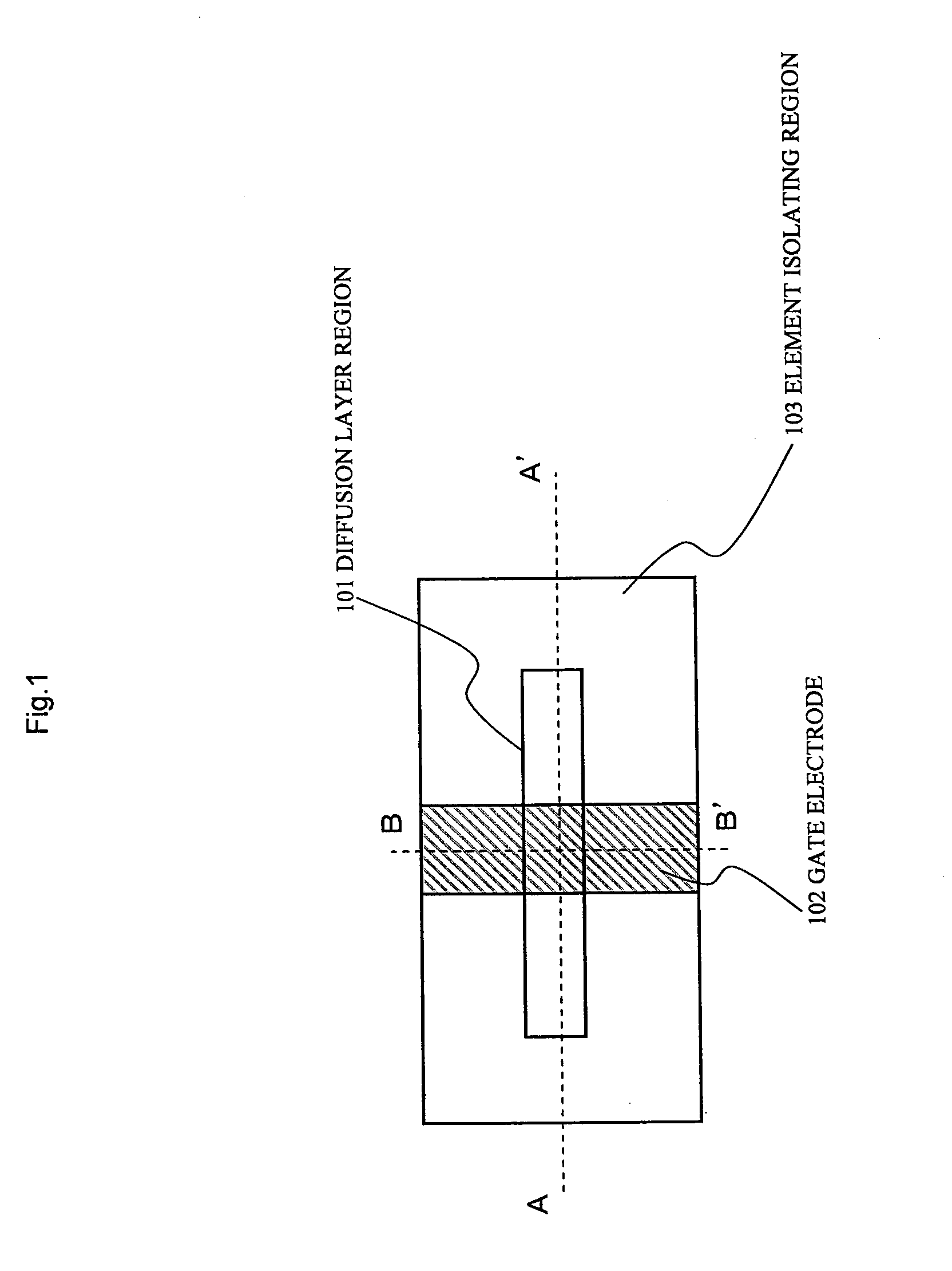
[0068]FIG. 3 is a plan view of an RC transistor having an SOI structure according to an embodiment of the present invention. Depictions of an electrode extraction wiring layer and the like have been omitted.

[0069]As shown in FIG. 3, an RC transistor having an SOI structure according to the present embodiment is provided with: element isolating regions 3 formed on a semiconductor substrate (not shown) made of silicon or the like; diffusion layer region (active region) 2 defined by element isolating region 3; gate electrode 5; and contact plugs 11.

[0070]Among diffusion layer region 2, both lateral portions that are not opposite to gate electrode 5 function as source / drain regions of the transistor.

[0071]Contact plugs 11 connect the source / drain regions with a wiring layer (not shown) provided on an upper layer thereof.

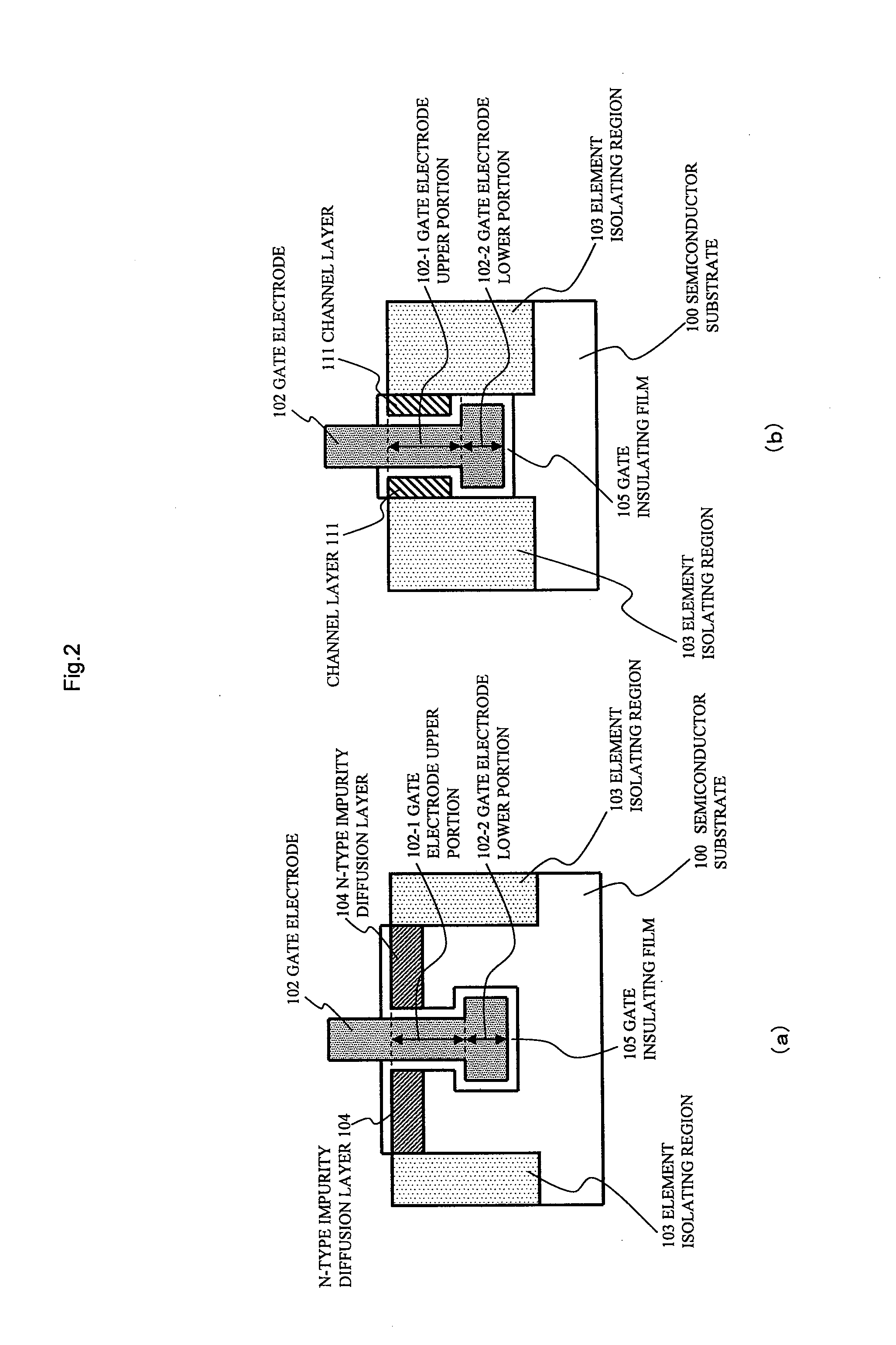
[0072]FIG. 4 shows cross-sectional views of the RC transistor having an SOI structure shown in FIG. 3, in which (a) is a cross-sectional view taken along line A-A′ of FI...

second embodiment

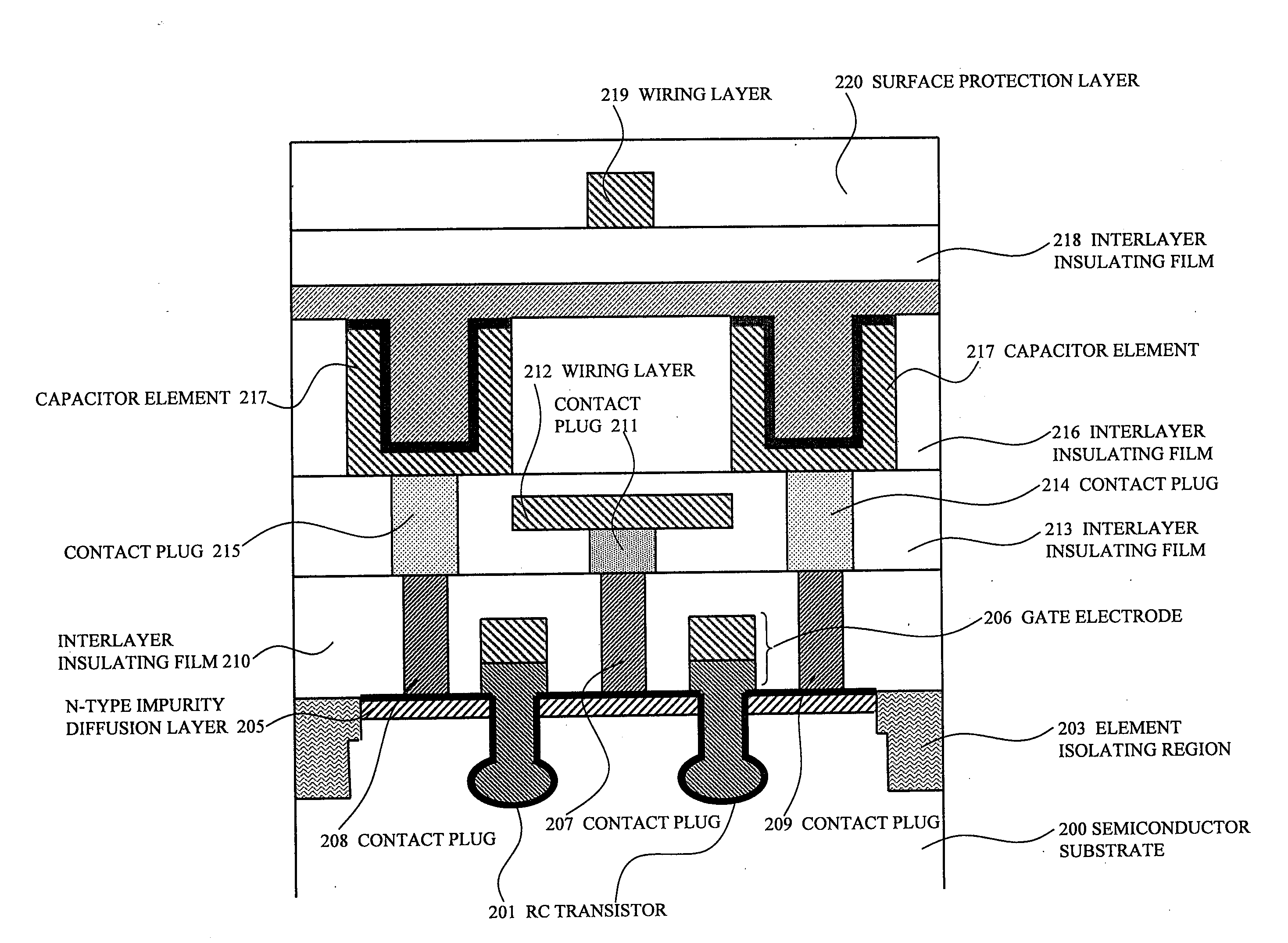
[0127]A case of applying the RC transistor having an SOI structure whose manufacturing method has been described in the first embodiment to a memory cell of a DRAM (Dynamic Random Access Memory) will be described below.

[0128]FIG. 21 is a plan view schematically showing a part of a DRAM memory cell that is a memory cell to which is applied a RC transistor having an SOI structure whose manufacturing method has been described in the first embodiment. Hereinafter, for the sake of simplicity, only portions related to the transistor will be described.

[0129]As shown in FIG. 21, plurality of diffusion layer regions (active regions) 204 is regularly disposed on a semiconductor substrate (not shown).

[0130]Each of a plurality of diffusion layer regions 204 is divided into a plurality of portions by a plurality of element isolating regions 203.

[0131]Element isolating regions 203 are formed by the method shown in the first embodiment described above. In addition, a plurality of gate electrodes 2...


PUM


Abstract

A semiconductor device provided with a field-effect transistor, the field-effect transistor including: a active region defined by element isolating region 3 formed on semiconductor substrate 1; gate electrode 5 provided so as to intersect the active region and having at least a part thereof embedded in a gate trench formed on semiconductor substrate 1; and SOI structure channel layer 4 formed in the active region so that one lateral face thereof is opposite to a part of gate electrode 5 embedded in the gate trench and the other lateral face thereof is in contact with a lateral face of element isolating region 3, wherein impurity diffusion layer 5 that functions as a source/drain region is disposed above channel layer 4, and impurity diffusion layer 9 and channel layer 4 are formed spaced apart from each other.

Description

[0001]This application is based upon and claims the benefit of priority from Japanese patent application No. 2008-161986, filed on Jun. 20, 2008, the disclosure of which is incorporated herein in its entirety by reference.BACKGROUND OF THE INVENTION[0002]1. Field of the Invention[0003]The present invention relates to a semiconductor device and a manufacturing method thereof and, in particular, to a semiconductor device including an RC transistor having an SOI structure and a manufacturing method thereof.[0004]2. Description of the Related Art[0005]In recent years, progress in miniaturization of semiconductor devices has necessitated reductions in the gate length of field-effect transistors (hereinafter described as transistors). A reduction in the gate length of a transistor brings the source and the drain of the transistor close to each other, thereby causing the effect of the drain to extend to the source. As a result, the threshold voltage of the transistor is problematically red...

Claims


Application Information

Patent Timeline
Patent Type & Authority Applications(United States)
IPC IPC(8): H01L27/108H01L21/8242
CPCH01L21/84H01L27/10876H01L29/785H01L27/1203H01L29/66795H01L27/10879H10B12/056H10B12/053
Inventor MIKASA, NORIAKI
Owner ELPIDA MEMORY INC
Why Eureka
Try Eureka