Semiconductor device and manufacture method thereof

a semiconductor and semiconductor technology, applied in the direction of semiconductor devices, electrical devices, transistors, etc., can solve the problems of increasing so as to prevent the deterioration of the characteristics of the memory cell tr, the parasitic capacitance of the gate electrode, and the effect of reducing the parasitic capacitan

Active Publication Date: 2009-08-18
MICRON TECH INC
View PDF14 Cites 27 Cited by
  • Summary
  • Abstract
  • Description
  • Claims
  • Application Information

AI Technical Summary

Benefits of technology

[0018]It is an object of the present invention to provide a semiconductor device of a trench gate type, which can be reduced in size and which can avoid short-channel effects in the trench gate type Tr.
[0036]The semiconductor device according to the present invention is provided with a trench gate Tr having a first gate electrode and a second gate electrode. A gate oxide film and the first gate electrode are formed in a lower part of a groove of the trench gate Tr. The top surface of the first gate electrode is located lower than the bottom surface of an impurity diffusion layer on the substrate interface, and higher than the distal end of a depletion layer formed in extension from the impurity diffusion layer. Groove side walls are formed on upper inner walls of the groove located upper than the first gate electrode so as to expose a central part of the top surface of the first gate electrode. The second gate electrode is provided to be in contact with a part of the top surface of the first gate electrode. The provision of a composite film consisting of the gate oxide film and the groove side wall between the gate electrode and the substrate in the upper part of the groove has an effect of reducing the parasitic capacitance of the gate electrode. Further, when the trench gate Tr of the present invention is used as a DRAM memory cell Tr, a DRAM memory cell having desirable device characteristics can be obtained which is capable of reducing the parasitic capacitance in the gate electrode, that is, the parasitic capacitance in word lines, and thereby preventing the deterioration in ON characteristics of the memory cell Tr without increasing the chip size.

Problems solved by technology

As described above, the short-channel effects of the memory cell Tr's have become more serious as the semiconductor device has been miniaturized.
In the trench gate Tr, however, the opposing area between the gate electrode and the substrate becomes inevitably wide.
This brings about increasing a parasitic capacitance of the gate electrode.
Therefore, when the trench gate Tr is employed as a DRAM memory cell Tr, the parasitic capacitance of a word line including the gate electrode will inevitably increase.
This may cause a problem of deterioration in the rise characteristics when the word line potential is turned ON.
Thus, the number of memory cells connected to each word line must be reduced, which disadvantageously results in an increase of a chip size.

Method used


Image

  • Semiconductor device and manufacture method thereof
  • Semiconductor device and manufacture method thereof
  • Semiconductor device and manufacture method thereof

Examples


Embodiment Construction

[0066]Exemplary embodiments of a semiconductor device and a manufacture method thereof according to the present invention will be described with reference to the accompanying drawings.

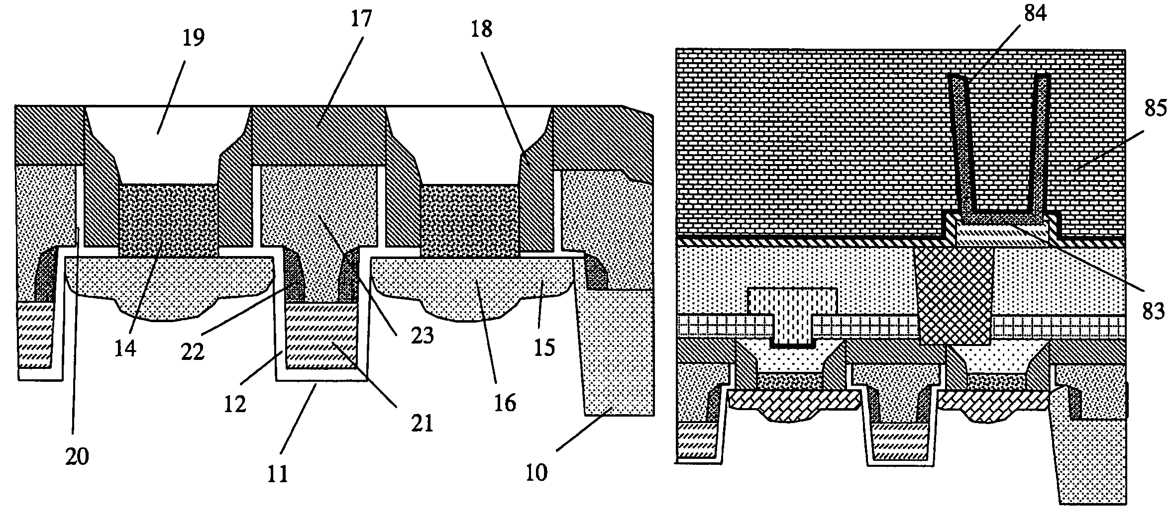
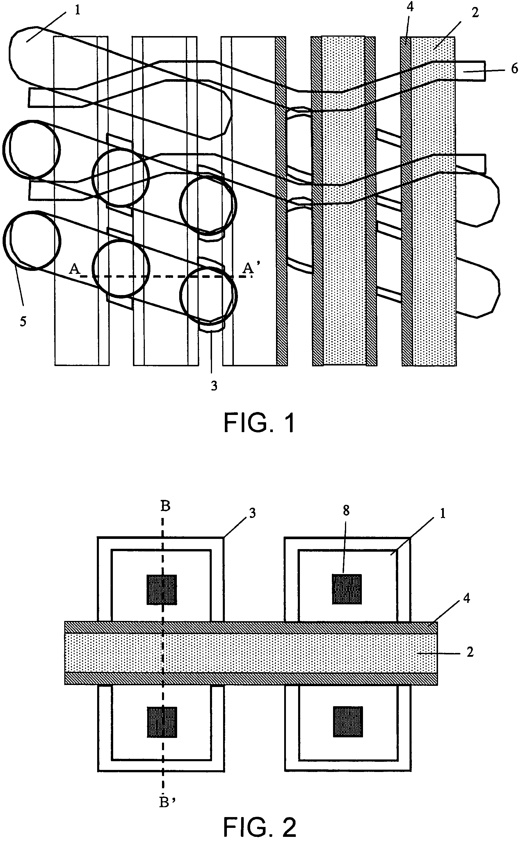
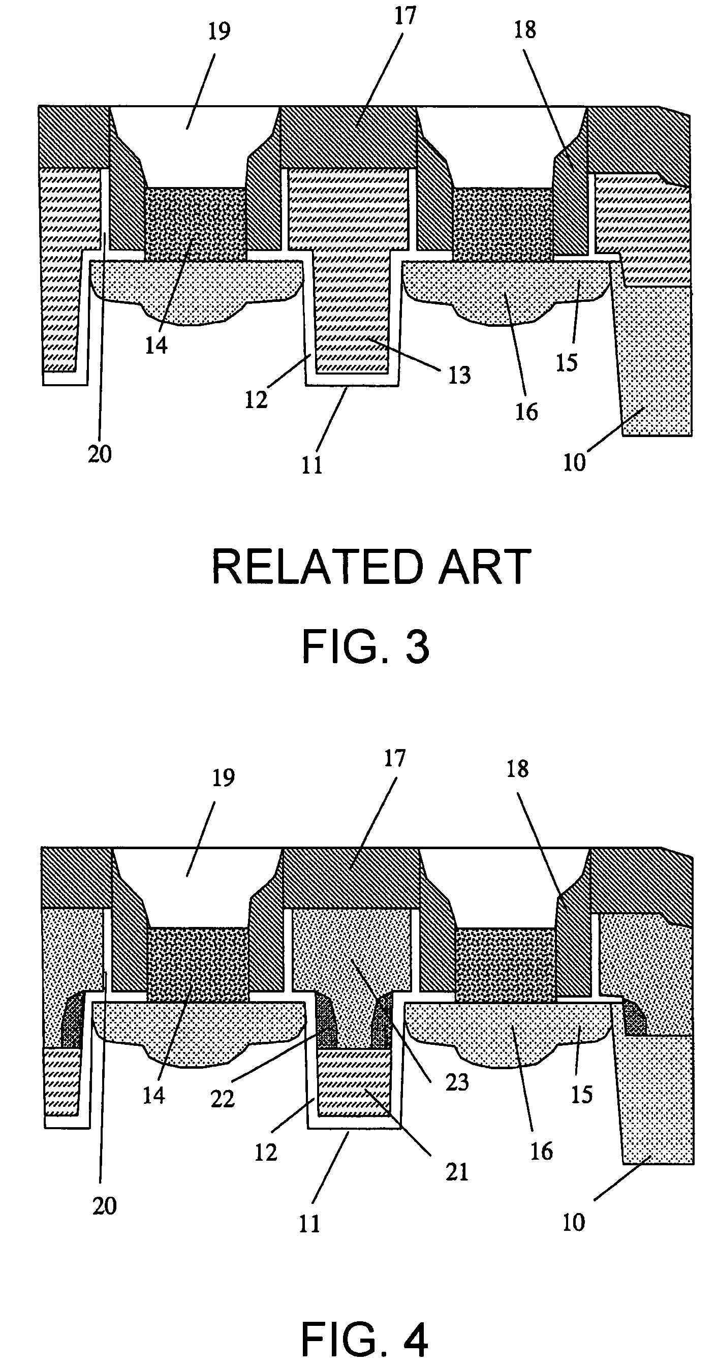
[0067]A semiconductor device according to a first embodiment of the invention can be specified by a DRAM memory cell and peripheral circuit Tr's as shown in FIGS. 1 and 2, respectively, but is different from FIG. 3 in a sectional view of the DRAM memory cell, as shown in FIG. 4 taken along a line A-A′ of FIG. 1. This is because the plan views of FIG. 1 and FIG. 2 show basic configurations, and these configurations are also applicable to the present invention also.

[0068]In FIG. 4, a trench gate Tr is illustrated and includes a groove 11 provided in a silicon substrate, a gate oxide film 12 formed on a portion including an inside surface of the groove 11, and a first gate electrode 21 formed on a part of the gate oxide film 12 located in the groove 11. Thus, the gate oxide film 12 is interposed between t...


PUM


Abstract

The present invention provides a trench gate Tr having a first gate electrode and a second gate electrode in the inside of a groove. The first gate electrode is provided in a groove lower part defining a channel of the Tr with a gate oxide film interposed between the first gate electrode and the substrate. The second gate electrode is provided in a groove upper part facing a Tr impurity diffusion layer, with a gate oxide film and a groove side wall film interposed between the second gate electrode and the groove upper part. The provision of the composite film consisting of the gate oxide film and the groove side wall between gate electrode and the substrate in the groove upper part enables reduction of the parasitic capacitance of the gate electrode.

Description

[0001]This application claims priority to prior application of JP 2006-172423, the disclosure of which is incorporated herein by reference.BACKGROUND OF THE INVENTION[0002]The present invention relates to a semiconductor device having a trench gate transistor and a manufacture method thereof.[0003]Semiconductor devices have made progress very fast in density, characteristic, and the like. Among the semiconductor devices, a DRAM (Dynamic Random Access Memory) device has been remarkably advanced. Herein, it is to be noted that the DRAM device includes DRAM cells arranged in a memory cell region and peripheral circuits arranged in a peripheral region.[0004]In such a DRAM device, the degree of integration of semiconductor elements, namely, DRAM cells has been increased substantially twice every one or two year. In order to achieve such high integration, the sizes of MOS (Metal-Oxide-Semiconductor) transistors have also been reduced. Such size reduction has entailed notable short-channel...

Claims


Application Information

Patent Timeline
Patent Type & Authority Patents(United States)
IPC IPC(8): H01L29/772H01L21/336
CPCH01L21/823437H01L27/10823H01L27/10876H01L27/10894H01L29/66621H01L29/42376H01L29/66553H01L27/10897H01L29/665H10B12/34H10B12/053H10B12/09H10B12/50
Inventor TANAKA, YOSHINORI
Owner MICRON TECH INC
Why Eureka
Try Eureka