Thin film circuit device, manufacturing method thereof, electro-optical apparatus, and electronic system

Inactive Publication Date: 2005-01-13
SEIKO EPSON CORP
View PDF1 Cites 34 Cited by
  • Summary
  • Abstract
  • Description
  • Claims
  • Application Information

AI Technical Summary

Benefits of technology

[0020] The lower connection electrode may be formed approximately flush with the underlayer. Hence, the bottom surface of the thin film circuit layer is planarized, and as a result, the lamination can be easily performed.
[0021] The

Problems solved by technology

However, wire connection between thin film circuits laminated

Method used


Image

  • Thin film circuit device, manufacturing method thereof, electro-optical apparatus, and electronic system
  • Thin film circuit device, manufacturing method thereof, electro-optical apparatus, and electronic system
  • Thin film circuit device, manufacturing method thereof, electro-optical apparatus, and electronic system

Examples


Embodiment Construction

[0038] Hereinafter, the exemplary embodiments of the present invention will be described with reference to drawings.

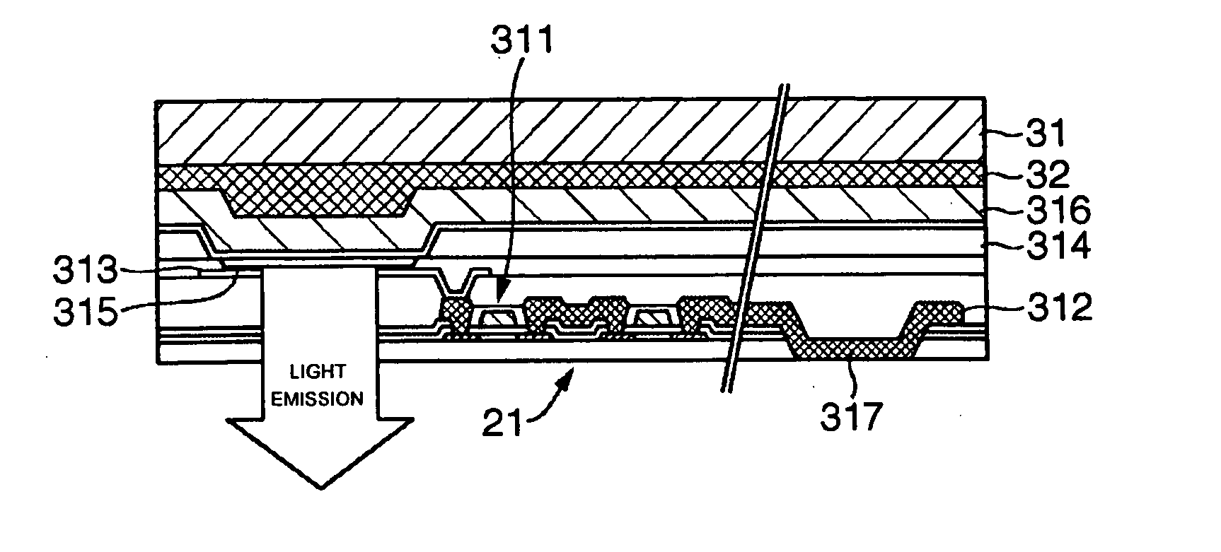
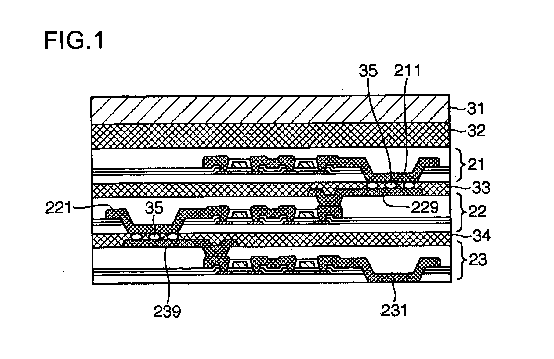
[0039] A thin film circuit device of an exemplary embodiment of the present invention has a structure in which thin film circuits are laminated to each other in the vertical direction, and in which, among the circuits mentioned above, an intermediate thin film circuit present inside the laminate is formed to have electrodes on the upper and the lower surfaces thereof for electrical connection. In addition, in the thin film circuit device according to the exemplary embodiment of the present invention, since an electrode is formed which is exposed at the rear surface of the thin film circuit, connection with a thin film circuit located thereunder and / or an exterior wire can be easily achieved.

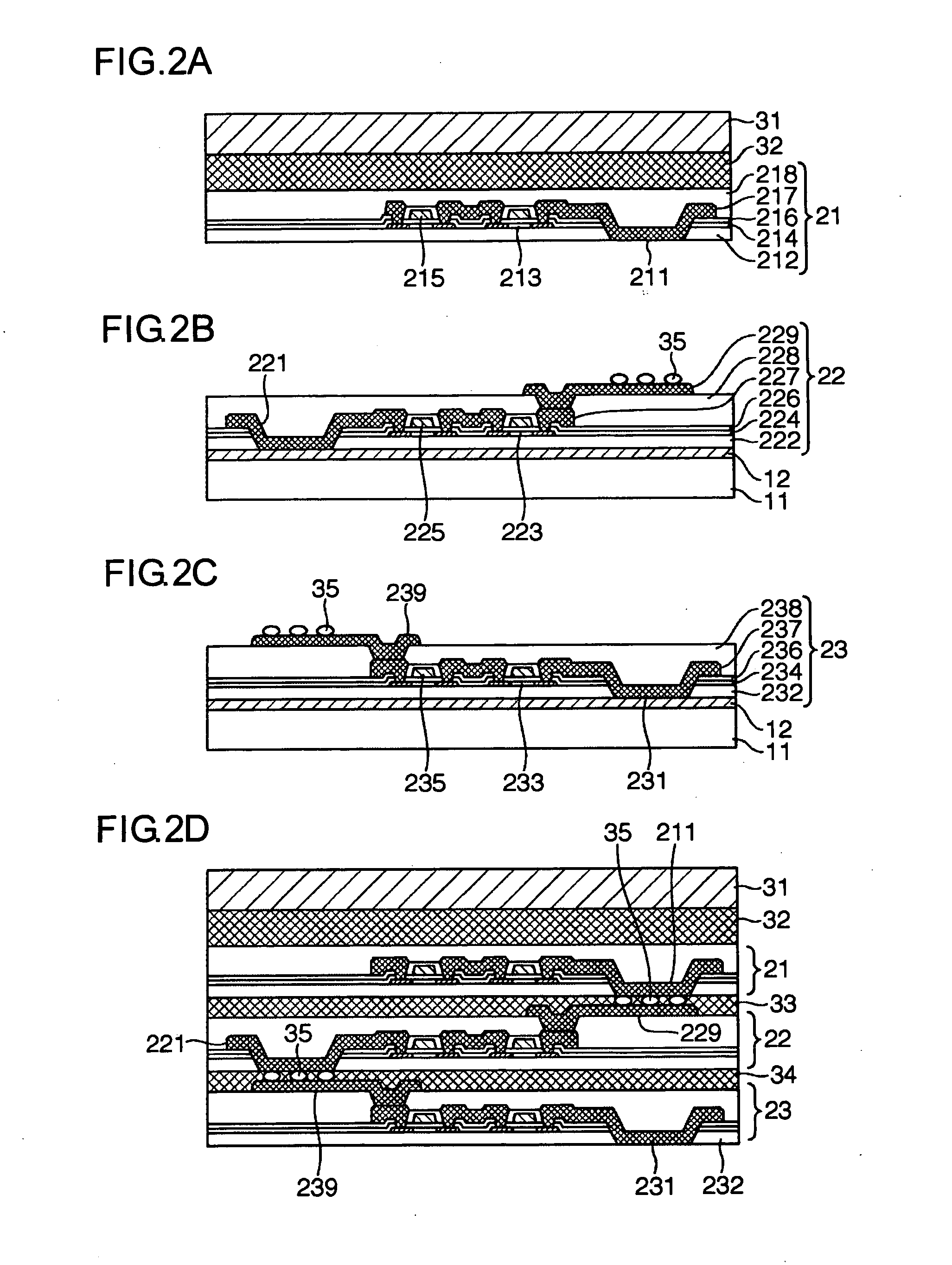
[0040] In a manufacturing method according to an exemplary embodiment of the present invention, a process to manufacture a thin film circuit device using a peeling and transferrin...


PUM


Abstract

To provide a thin film circuit device in which a three-dimensional circuit structure is realized, a thin film circuit device is formed of a first thin film circuit layer and a second thin film circuit layer laminated to each other. The first thin film circuit layer contains a first thin film circuit provided between an underlayer and a protective layer and a lower connection electrode connected to the first thin film circuit and exposed at a part of the bottom surface of the underlayer. The second thin film circuit layer contains a second thin film circuit provided between an underlayer and a protective layer, an upper connection electrode connected to the second thin film circuit and exposed at a part of the top surface of the protective layer, and a lower connection electrode connected to the second thin film circuit and exposed at a part of the bottom surface of the underlayer. The first and the second thin film circuits are bonded to each other so that the lower connection electrode of the first thin film circuit layer is electrically connected to the upper electrode of the second thin film circuit layer.

Description

BACKGROUND OF THE INVENTION [0001] 1. Field of Invention [0002] The present invention relates to thin film circuit devices having a three-dimensional thin film circuit and to methods to manufacture a thin film circuit device having a three-dimensional circuit structure. [0003] 2. Description of Related Art [0004] In semiconductor devices and the like, since high temperature processes and the like are performed when necessary layers and regions are formed on a substrate to form a laminate, selection of members to form substrates and laminates may be restricted in some cases. For example, resin films, plastic substrates, and the like are not suitable in a high temperature process. [0005] Hence, for example, according to Japanese Unexamined Patent Application Publication No. 2002-217391, a peeling and transferring technique has been proposed in which a thin film circuit is formed above a heat resistant first substrate with an isolation layer provided therebetween. A non-heat resistant ...

Claims


Application Information

Patent Timeline
IPC IPC(8): G02F1/1345G02F1/136G09F9/30H01L21/02H01L21/336H01L21/768H01L21/77H01L21/8238H01L21/84H01L23/52H01L27/00H01L27/08H01L27/092H01L27/12H01L29/786H01L51/50
CPCH01L27/1266H01L27/124H01L2221/68363H01L2224/32145H01L2224/83001G02F1/136
Inventor UTSUNOMIYA, SUMIO
Owner SEIKO EPSON CORP
Why Eureka
Try Eureka