Susceptor and deposition apparatus including the same

a deposition apparatus and susceptor technology, applied in the direction of chemically reactive gases, coatings, crystal growth processes, etc., can solve the problems of affecting the yield and reliability of the semiconductor device, defects such as d-effect defects, crystal original particles, etc., and achieve the effect of minimizing the physical impact between the susceptor and the wafer

Inactive Publication Date: 2005-01-27
SAMSUNG ELECTRONICS CO LTD
View PDF6 Cites 195 Cited by
  • Summary
  • Abstract
  • Description
  • Claims
  • Application Information

AI Technical Summary

Benefits of technology

[0019] According to the present invention, although the wafer may come into contact with the susceptor during the deposition process, the ductile stress-reducing bumper

Problems solved by technology

The quality of a silicon wafer used as a substrate in the fabricating of a highly integrated semiconductor device greatly affects the yield and reliability of the semiconductor device.
However, defects such as a D-effect defect, crystal original particles (COPs) and a conductive oxide are frequently generated during the fabricating of the silicon wafer.
As a result, a slip dislocation may occur in the silicon wafer when the wafer experiences even a small physical impact.
The slip dislocation is caused by silicon atoms slipping

Method used


Image

  • Susceptor and deposition apparatus including the same
  • Susceptor and deposition apparatus including the same
  • Susceptor and deposition apparatus including the same

Examples


Embodiment Construction

[0028] The present invention now will be described more fully hereinafter with reference to the accompanying drawings.

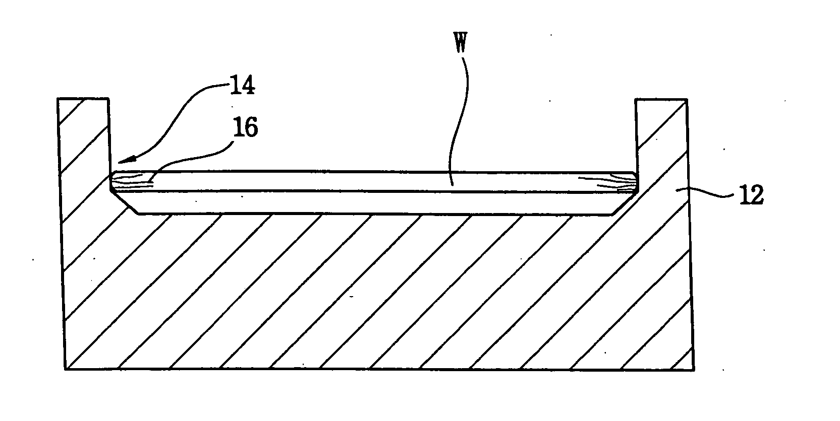
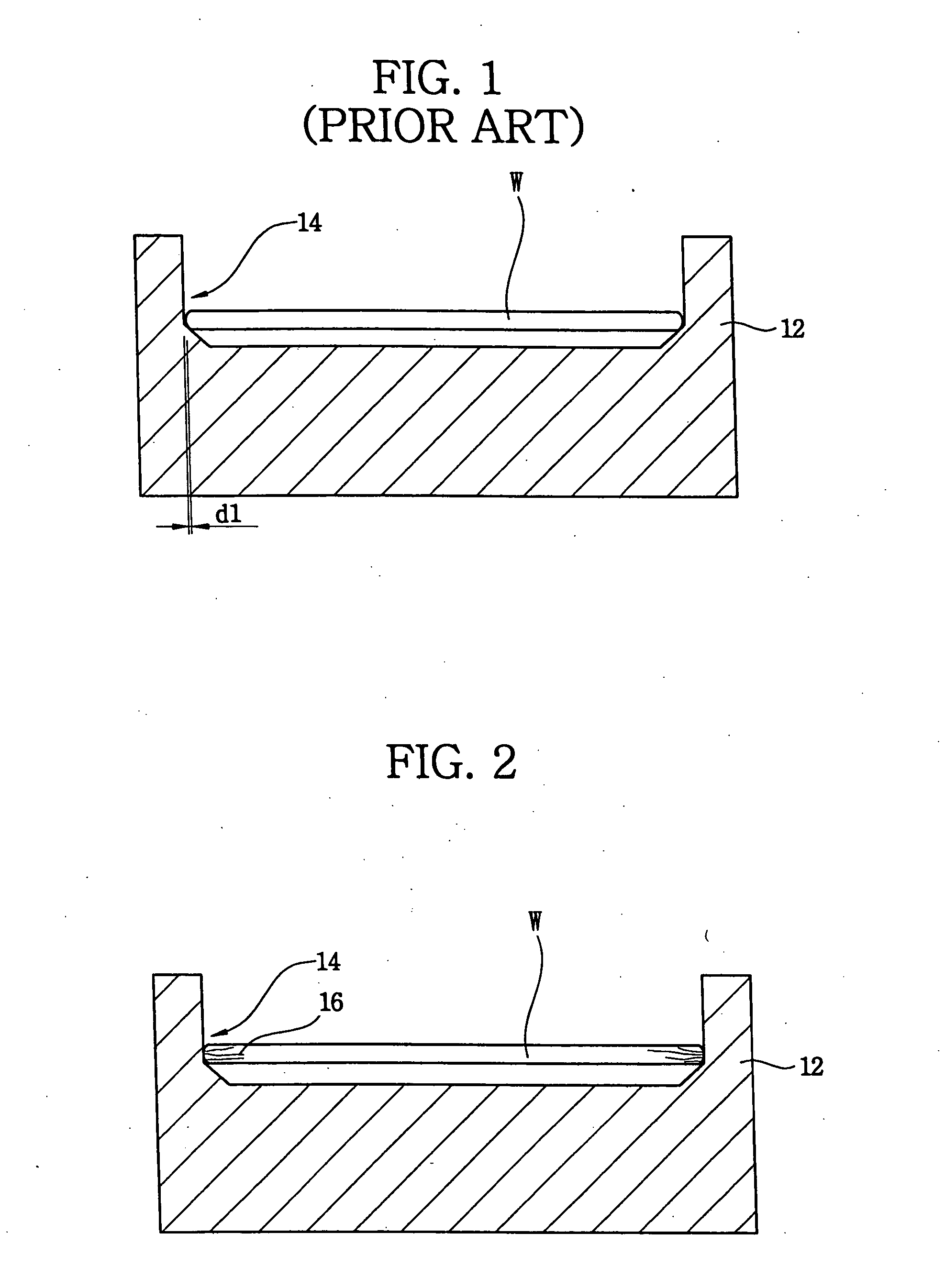
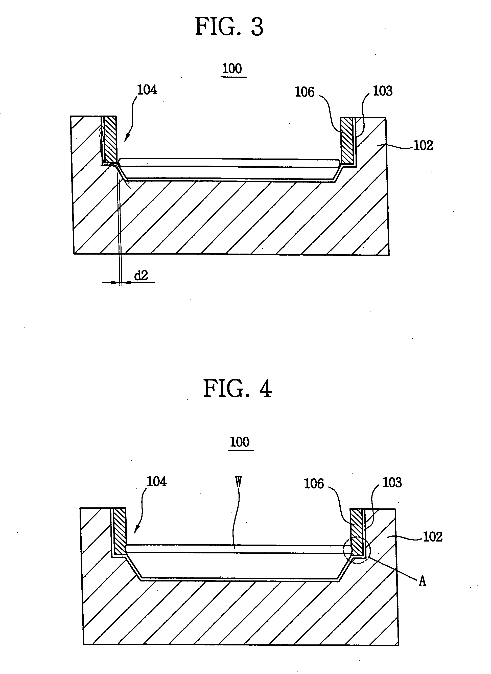
[0029] Referring now to FIG. 3, a susceptor 100 is provided in a deposition chamber. The susceptor 100 includes a plate 102. The plate 102 has a recess 104 in an upper portion thereof. A wafer W is received in the recess 104 during a process in which a layer is formed on the wafer.

[0030] The plate 102 may have only one recess 104 in the upper portion thereof. Alternatively, as shown in FIG. 6, the plate 102 may have a plurality of recesses 104 each configured to accommodate a respective wafer W. Preferably, the recesses 104 each have a circular sectional shape in a plane parallel to the upper surface of the plate 12, and are spaced from one another in that plane or lie tangentially with respect to one another as shown in the figure. Thus, layers may be simultaneously formed on a plurality of the wafers W when the susceptor 100 of FIG. 6 is employed in the depositio...


PUM

PropertyMeasurementUnit
Temperatureaaaaaaaaaa
Thicknessaaaaaaaaaa
Angleaaaaaaaaaa

Abstract

A susceptor for use in a deposition apparatus includes a recess in which a wafer is received, and a stress-reducing bumper disposed along the side of the recess. The stress-reducing bumper is of material having ductility at a relatively high temperature. Therefore, when the wafer contacts the stress-reducing bumper, such as may occur due to thermal expansion of the wafer during processing, the force of the impact on the wafer is minimized by an elastic deformation of the stress-reducing bumper. As a result, defects, such as slip dislocations at the outer peripheral edge of the wafer, are prevented.

Description

BACKGROUND OF THE INVENTION [0001] 1. Field of the Invention [0002] The present invention relates to a susceptor of a deposition apparatus. More particularly, the present invention relates to a susceptor used in a chemical vapor deposition apparatus for forming an epitaxial layer. [0003] 2. Description of the Related Art [0004] The quality of a silicon wafer used as a substrate in the fabricating of a highly integrated semiconductor device greatly affects the yield and reliability of the semiconductor device. The quality of the silicon wafer is dependent on the distribution and density of internal or external defects such as those generated on a surface of the silicon wafer during the manufacturing of the silicon wafer. [0005] Generally, a silicon wafer is fabricated as follows. First, a polycrystalline silicon ingot is formed. The polycrystalline silicon ingot is grown by a Czochoralski (CZ) method or a floating zone (FZ) method to form a single crystalline silicon ingot. The singl...

Claims


Application Information

Patent Timeline
IPC IPC(8): C23C16/00H01L21/205C23C16/458C30B25/12C30B31/14
CPCC23C16/4584C30B31/14C30B25/12H01L21/205
Inventor KANG, TAE-SOOCHOI, SOO-YEOLCHO, KYOO-CHULKIM, GI-JUNGKIM, JIN-HOHEO, TAE-YEOL
Owner SAMSUNG ELECTRONICS CO LTD
Why Eureka
Try Eureka