Wafer support pin for preventing slip dislocation during annealing of water and wafer annealing method using the same

a technology of annealing method and support pin, which is applied in the field of wafer support pin, can solve the problems of deteriorating yield, increasing the weight of wafers, and reducing the service life of wafers, so as to minimize gravitational stress and heat loss, improve the structure, and minimize the effect of slip dislocation

Active Publication Date: 2010-08-03
LG SILTRON
View PDF6 Cites 0 Cited by
  • Summary
  • Abstract
  • Description
  • Claims
  • Application Information

AI Technical Summary

Benefits of technology

[0008]The present invention is designed to solve the problems of the prior art, and therefore it is an object of the present invention to provide a wafer support pin having an improved structure to minimize gravitational stress and heat loss, thereby capable of minimizing slip dislocation; and a wafer annealing method using the same.
[0009]In order to accomplish the above object, in one aspect of the present invention, there is provided a wafer support pin, wherein a front end of the wafer support pin, contacted with the wafer, is flat or rounded to minimize gravitational stress during annealing the wafer.
[0011]In case at least the front end of the wafer support pin is made of silicon material, the monocrystalline or polycrystalline silicon may be doped with N or C to enhance mechanical strength. In addition, at least the front end of the wafer support pin may be surface-coated with SiC or Si3N4 to enhance abrasion resistance of the wafer support pin.

Problems solved by technology

The high temperature rapid thermal annealing anneals a wafer for several to several ten seconds at a high temperature of 1,150 to 1,250° C., which inevitably causes slip dislocation in the wafer.
If slip dislocation generated during the high temperature annealing exists on a surface, current leakage occurs in the semiconductor device manufacturing procedure, which becomes a cause of deteriorated yield.
However, as wafers become larger, weight of wafer also tends to become greater.
Thus, the gravitational stress, which was not issued in 8-inch wafer, becomes a problem in 12-inch wafer, as explained later, so the conventional wafer supporting method is now insufficient for slip control.

Method used


Image

  • Wafer support pin for preventing slip dislocation during annealing of water and wafer annealing method using the same
  • Wafer support pin for preventing slip dislocation during annealing of water and wafer annealing method using the same
  • Wafer support pin for preventing slip dislocation during annealing of water and wafer annealing method using the same

Examples


Embodiment Construction

[0028]Hereinafter, preferred embodiments of the present invention will be described in detail with reference to the accompanying drawings.

[0029]Prior to the description, it should be understood that the terms used in the specification and the appended claims should not be construed as limited to general and dictionary meanings, but interpreted based on the meanings and concepts corresponding to technical aspects of the present invention on the basis of the principle that the inventor is allowed to define terms appropriately for the best explanation. Therefore, the description proposed herein is just a preferable example for the purpose of illustrations only, not intended to limit the scope of the invention, so it should be understood that other equivalents and modifications could be made thereto without departing from the spirit and scope of the invention.

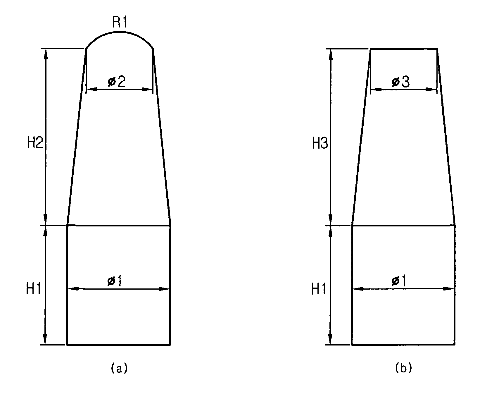
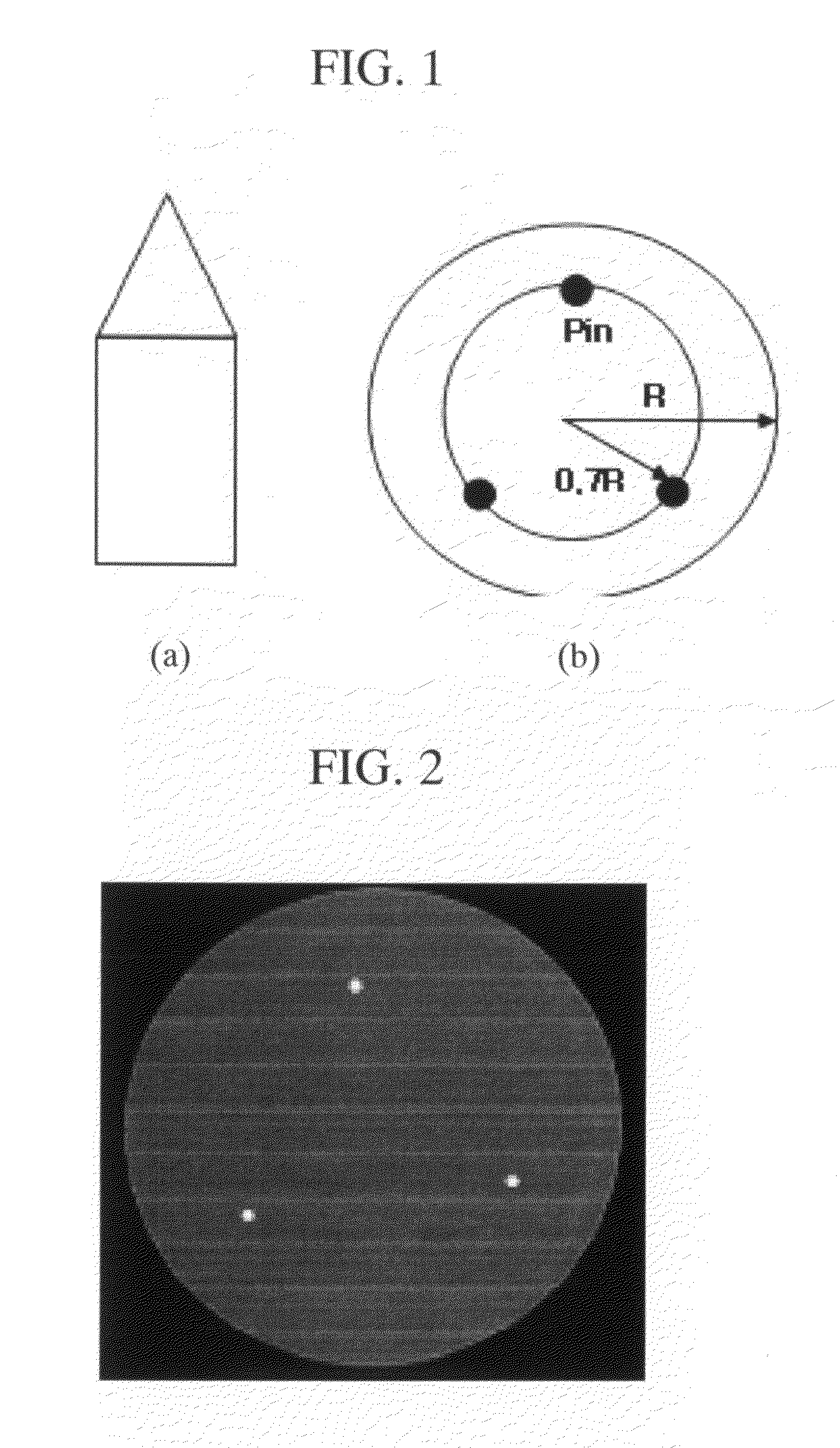
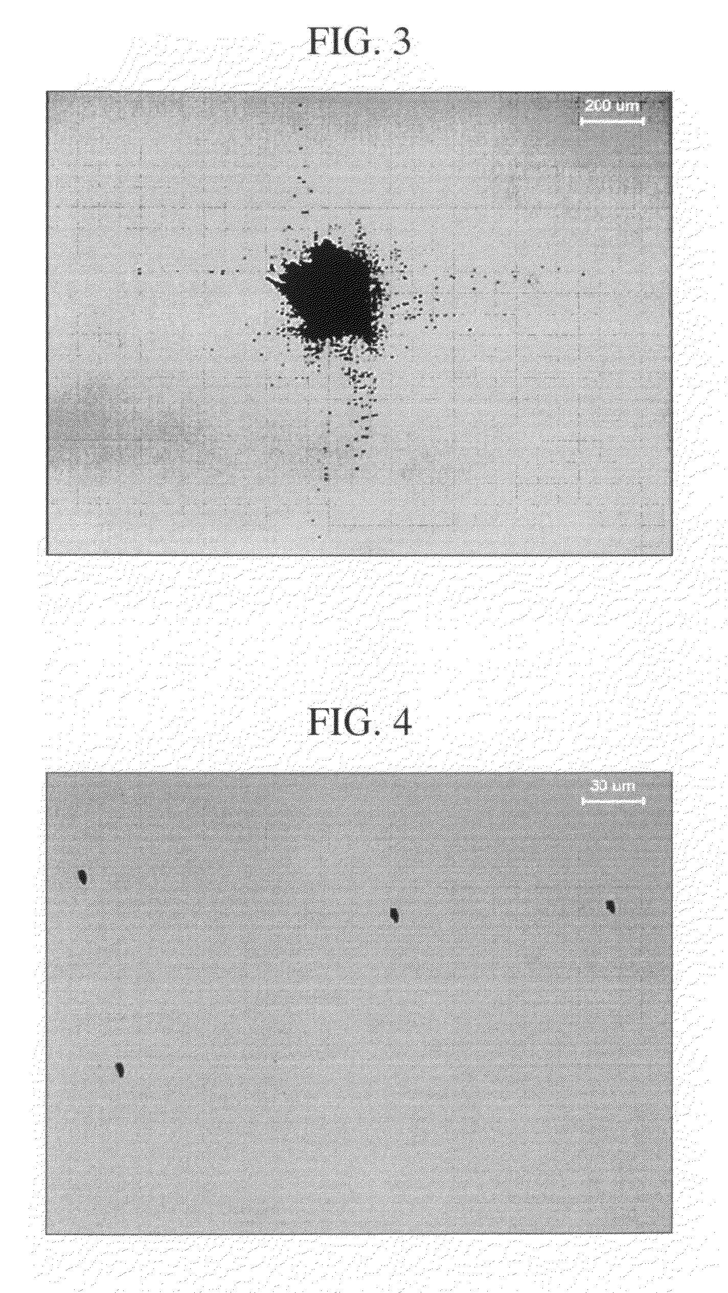
[0030]Prior to explaining a wafer support pin according to the present invention, an analysis result after rapid thermal annealin...


PUM

PropertyMeasurementUnit
lengthaaaaaaaaaa
diameteraaaaaaaaaa
diameteraaaaaaaaaa

Abstract

A wafer support pin has a front end contacted with a wafer such that the front end is flat or rounded. Thus, gravitational stress is minimized during annealing the wafer, thereby minimizing slip dislocation. This wafer support pin is suitably used for annealing of a wafer, particularly high temperature rapid thermal annealing of a large-diameter wafer.

Description

BACKGROUND OF THE INVENTION[0001]1. Field of the Invention[0002]The present invention relates to a wafer support pin used in annealing a wafer and a wafer annealing method using the same, and more particularly to a structure of a wafer support pin capable of minimizing gravitational stress applied to a wafer and also capable of minimizing heat loss to minimize slip dislocation, and a wafer annealing method using the same.[0003]2. Description of the Related Art[0004]An annealing process is generally carried during a semiconductor device manufacturing procedure. In case of a silicon wafer, oxygen existing in the wafer forms oxygen precipitates during the annealing process conducted in the semiconductor device manufacturing procedure. Also, during the semiconductor device manufacturing procedure, oxygen precipitates exceeding a certain level act as internal gettering sites against metal impurities that may be a contamination source, so the oxygen precipitates are inevitable essential e...

Claims


Application Information

Patent Timeline
Patent Type & Authority Patents(United States)
IPC IPC(8): H01L21/26
CPCH01L21/6875H01L21/68757H01L21/324H01L21/683
Inventor KIM, KUNHONG, JIN-KYUNSEO, WOO-HYUNSONG, KYOUNG-HWAN
Owner LG SILTRON
Why Eureka
Try Eureka