

Plasma display panel
- Summary
- Abstract
- Description
- Claims
- Application Information
AI Technical Summary
Benefits of technology
Problems solved by technology
Method used
Image

Examples
first embodiment
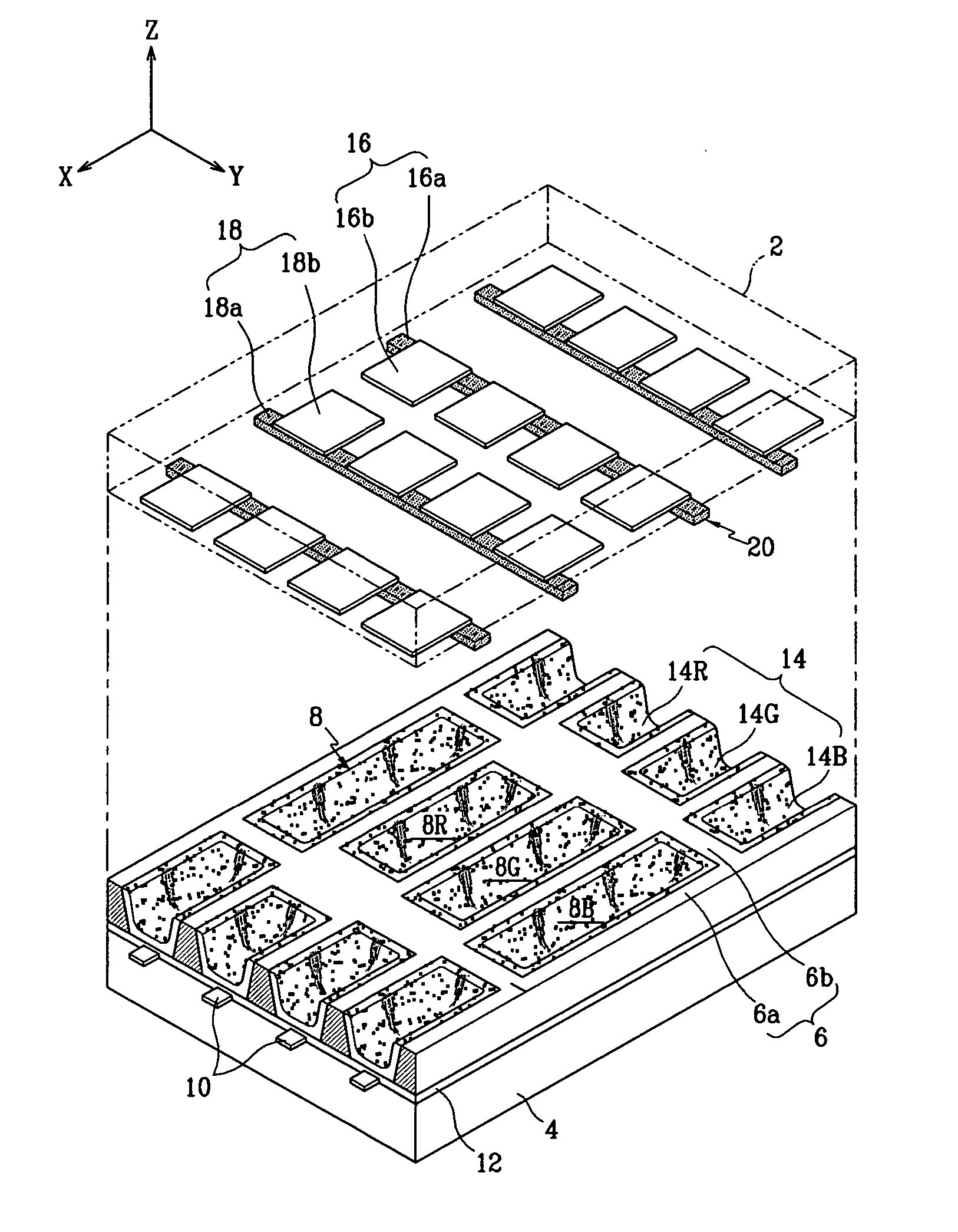
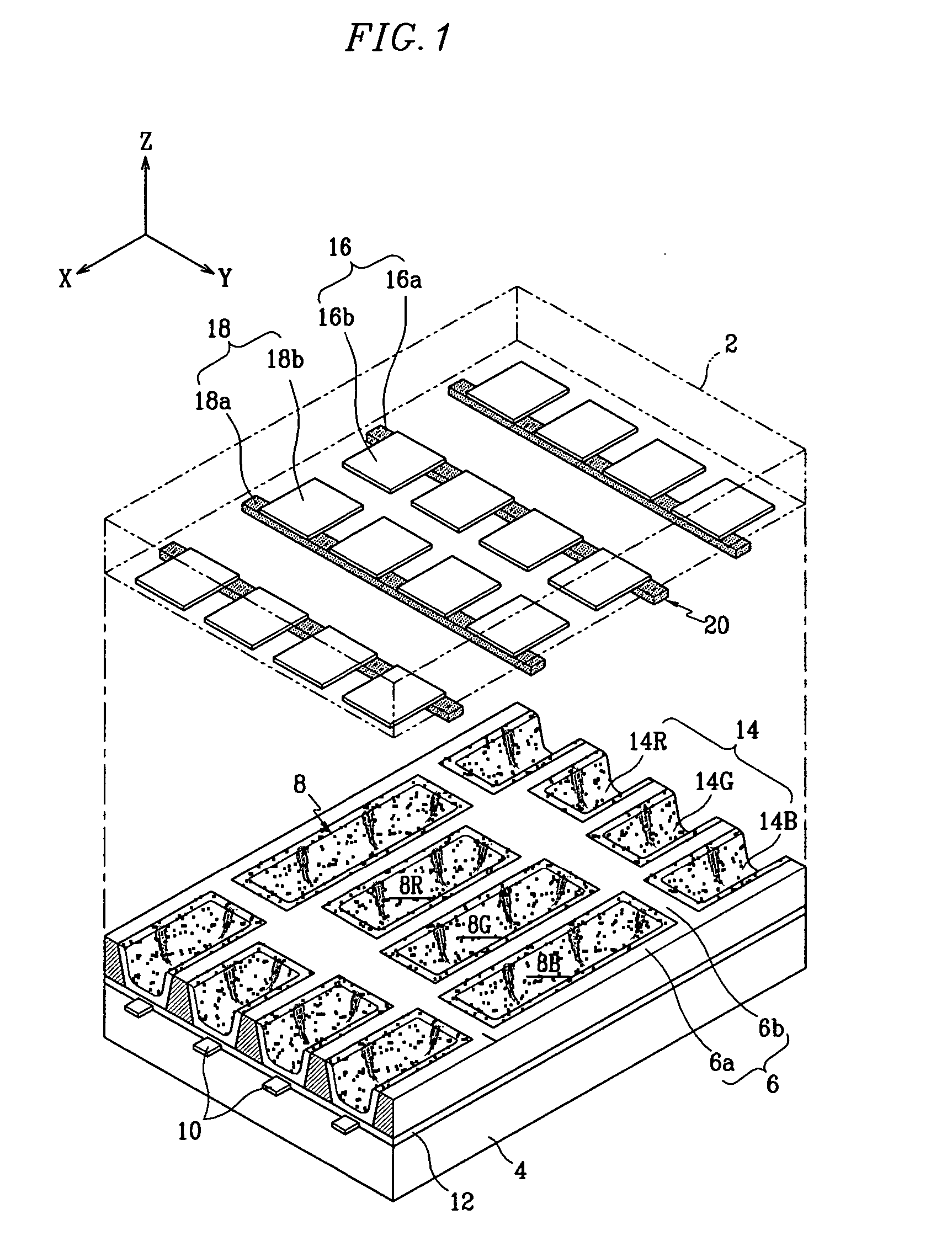
[0047]FIG. 1 is a partial exploded perspective view of a plasma display panel according to the present invention, and FIG. 2 is a partial plan view of the plasma display panel of FIG. 1.
[0048] A plasma display panel (PDP) according to the first embodiment includes first substrate 2 and second substrate 4 provided substantially in parallel with a predetermined gap therebetween. Barrier ribs6 define discharge cells 8 between first substrate 2 and second substrate 4. Independent discharge taking place in each of the discharge cells 8 results in the emission of visible light for the display of color images.
[0049] In more detail, address electrodes 10 are formed along one direction (direction X in the drawings) on a surface of second substrate 4 opposing first substrate 2. Dielectric layer 12 is formed over an entire surface of second substrate 4 covering address electrodes 10. As an example, address electrodes 10 are formed in a uniform, stripe pattern with a predetermined interval the...
third embodiment
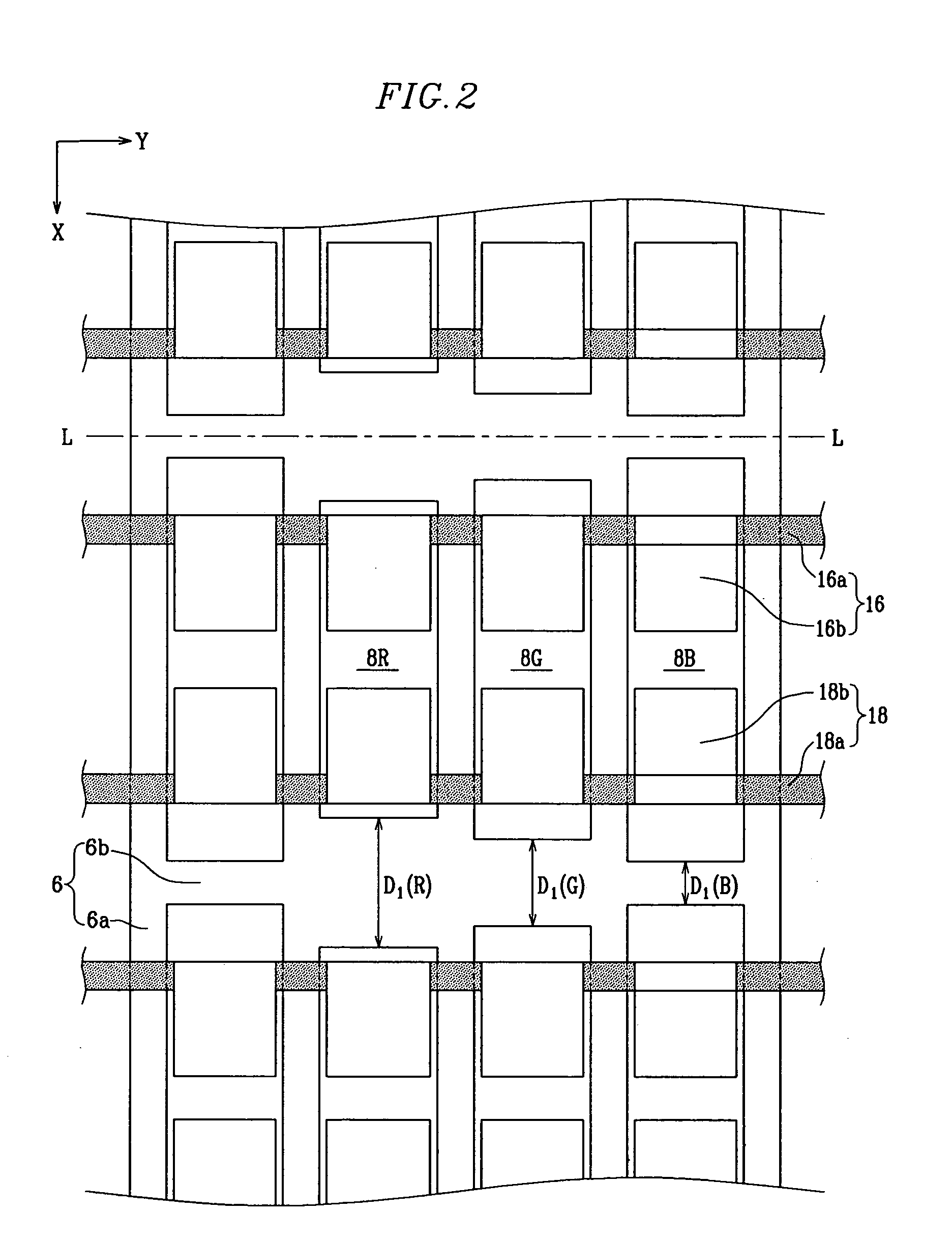
[0067] In the third embodiment, each of the discharge cells 8R, 8G, 8B is formed as rectangular islands surrounded by first barrier rib members 6a and second barrier rib members 6b. Further, distances between first barrier rib members 6a adjacent in direction Y are substantially identical, that is, widths of discharge cells 8 along direction Y are substantially identical. However, distances between second barrier rib members 6b adjacent in direction X vary in such a manner that red, green, and blue discharge cells 8R, 8G, 8B have different volumes. In particular, discharge cells 8 satisfy the following condition.
D4(R)4(G)4(B) [Formula 4][0068] where D4(R) is a length of red discharge cells 8R along the direction of address electrodes 10, D4(G) is a length of green discharge cells 8G along the direction of address electrodes 10, and D4(B) is a length of blue discharge cells 8B along the direction of address electrodes 10.
[0069] If horizontal lines H are drawn along the direction su...
second embodiment
[0071] With the formation of a single non-discharge cell 24 common to adjacent rows of discharge cells 8 as described above, the overall volume of non-discharge cells 24 may be increased such that heat-emitting effects are further increased over the
PUM
 Abstract
Description
Claims
Application Information