Circuit board testing apparatus and method for testing a circuit board
- Summary
- Abstract
- Description
- Claims
- Application Information
AI Technical Summary
Benefits of technology
Problems solved by technology
Method used
Image

Examples
first embodiment
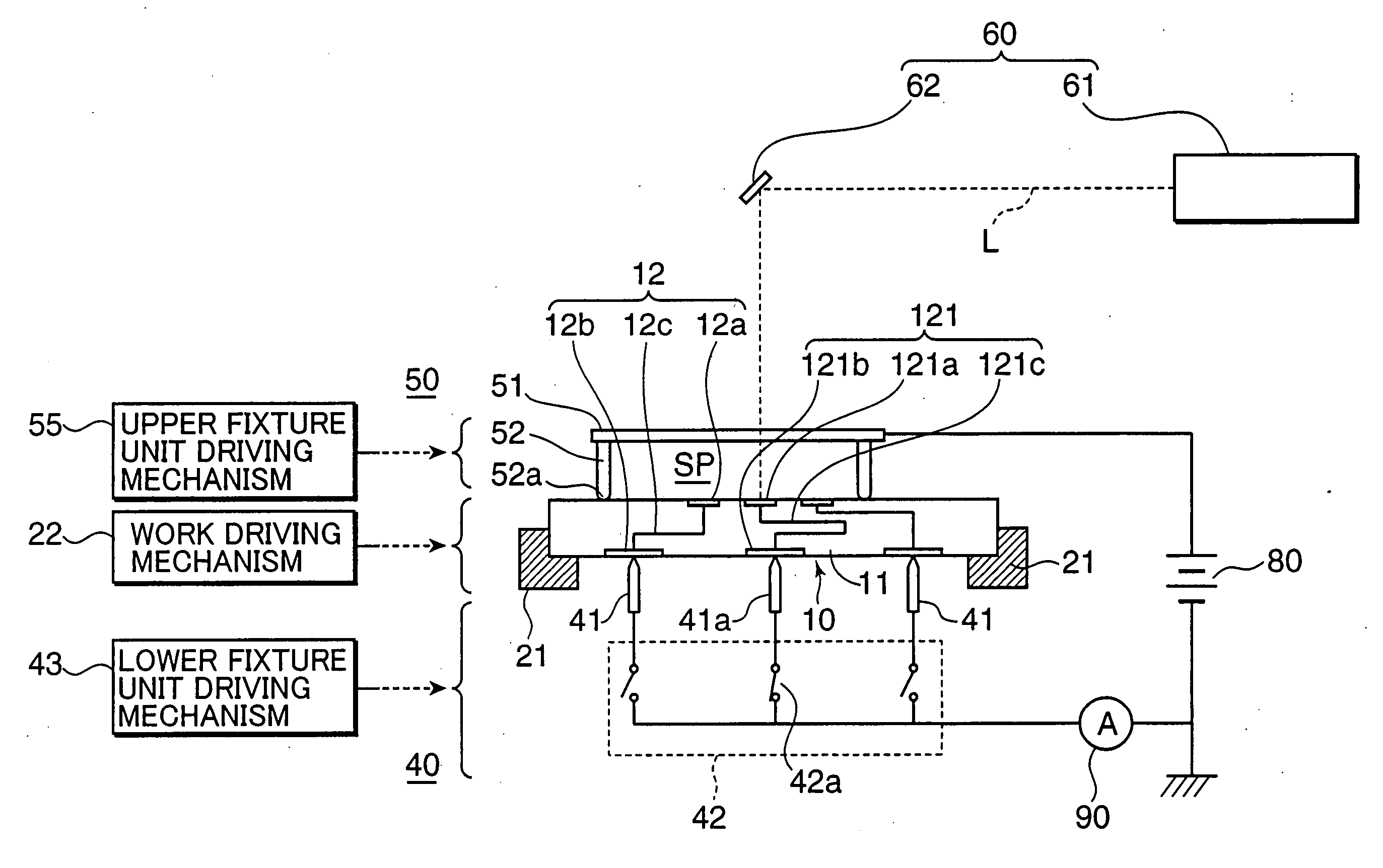
Referring to FIGS. 1 and 2 showing a circuit board testing apparatus in accordance with the invention, a circuit board testing apparatus is adapted to test a circuit board 10 on which a semiconductor chip is to be mounted according to C4 (Controlled Collapse Chip Connection) package method.
As shown in FIG. 1, the circuit board 10 is formed with a number of wirings 12, 121, 122 on a base plate 11. Each wiring 12, 121 or 122 includes a pad portion 12a, 121a or 122a which is formed on one or upper surface of the base plate11 in correspondence to a pad portion to which a semiconductor chip is connected, a ball grid portion 12b, 121b or 122b which is formed on the opposite or bottom surface of the base plate 11, and a conductive portion 12c which extends through the base plate 11 to electrically connect the pad portion 12a, 121a or 122a and the ball grid portion 12b, 121b or 122b. (For the simplicity of explanation, description will be made from now on with reference to the pad portion ...
second embodiment
Next, an operation of the circuit board testing apparatus in accordance with the second embodiment is described with reference to FIG. 11. FIG. 11 is a flowchart showing operations of the testing apparatus shown in FIG. 8. When an untested work (circuit board) 210 is loaded on the lower fixture unit 240 positioned at a load / unload position by a handling device (not shown) incorporated in the testing apparatus or a manual operation by an operator (in Step T1), the controller 201 start to control operations of the various parts of the apparatus to execute the following steps T2 to T11 so as to test shorts and open-circuits in the work 210.
When the work 210 is loaded on the lower fixture unit 240, the lower fixture unit 240 is moved to the test position while carrying the work 210 thereon (in Step T2). Thus, the work 210 is positioned at the test position. Then, the metallic plate 241 is brought into contact with the conductive probe 281 to be connected to the current detecting sectio...
third embodiment
FIG. 17 is a diagram showing a circuit board testing apparatus in accordance with the invention. FIG. 18 is a block diagram showing an electric configuration of the testing apparatus in FIG. 17. A circuit board testing apparatus is adapted to test a circuit board 410 which is capable of mounting thereon a semiconductor chip according to C4 (Controlled Collapse Chip Connection) package method.
As shown in FIG. 17, the circuit board 410 is constructed in such a manner that a plurality of wirings as represented by the wiring 412 are formed on a base plate 411. Each wiring 412 includes a pad portion 412a formed on one surface of the base plate 411 to be connected with a pad on a semiconductor chip, a ball grid portion 412b formed on the opposite surface of the base plate 411, and a conductive portion 412c arranged on or in the base plate 411 to electrically connect the pad portion 412a and the ball grid portion 412b. The pad portions 412a are arranged at small pitches to correspond to t...
PUM
 Abstract
Description
Claims
Application Information
 - R&D Engineer
- R&D Manager
- IP Professional
- Industry Leading Data Capabilities
- Powerful AI technology
- Patent DNA Extraction
Browse by: Latest US Patents, China's latest patents, Technical Efficacy Thesaurus, Application Domain, Technology Topic.
© 2024 PatSnap. All rights reserved.Legal|Privacy policy|Modern Slavery Act Transparency Statement|Sitemap