

Array substrate having double-layered metal patterns and method of fabricating the same
a metal pattern and substrate technology, applied in non-linear optics, instruments, optics, etc., can solve the problems of affecting the image quality of the liquid crystal display device, affecting the degree of image quality, and affecting the stability of the substrate, so as to increase the manufacturing yield and increase the manufacturing process stability
- Summary
- Abstract
- Description
- Claims
- Application Information
AI Technical Summary
Benefits of technology
Problems solved by technology
Method used
Image

Examples
Embodiment Construction
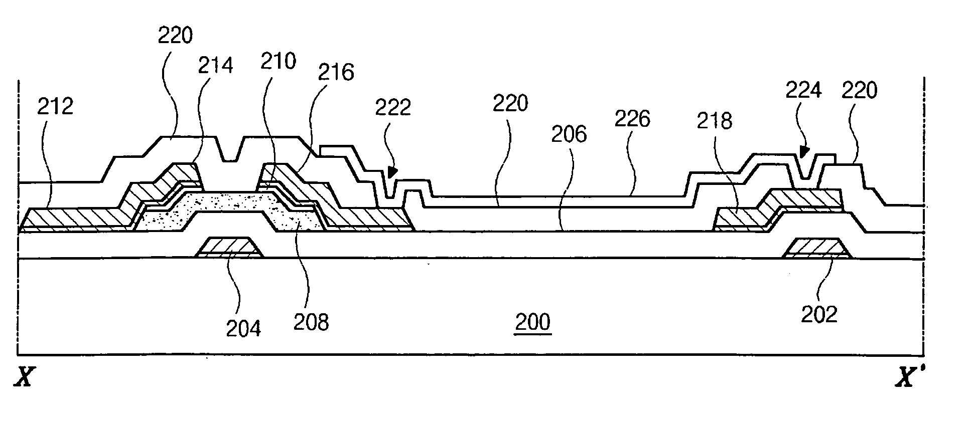
[0046] Reference will now be made in detail to the illustrated embodiments of the present invention, examples of which are illustrated in the accompanying drawings. Wherever possible, the same reference numbers will be used throughout the drawings to refer to the same or like parts.
[0047]FIG. 7 is a photograph of partially-etched copper / molybdenum-alloy (Cu / Mo-alloy) double layers taken by a Scanning Electron Microscope (SEM). FIG. 8 is an enlarged view showing a portion of the etched copper / molybdenum-alloy (Cu / Mo-alloy) double layers of FIG. 7.
[0048] As shown in FIGS. 7 and 8, a molybdenum alloy (Mo-alloy) layer 102 is first formed on a substrate 100 and then a copper (Cu) layer 104 is sequentially formed on the molybdenum alloy (Mo-alloy) layer 102. Thereafter, the Mo-alloy layer 102 and the Cu layer 104 are patterned to form a Cu / Mo-alloy double-layered metal pattern. After patterning, a surface of the substrate 100 is smoothed, as indicated in FIG. 7. The Mo-alloy layer 102 i...
PUM
| Property | Measurement | Unit |
|---|---|---|
| thickness | aaaaa | aaaaa |
| thickness | aaaaa | aaaaa |
| thickness | aaaaa | aaaaa |
Abstract
Description
Claims
Application Information