Liquid crystal display panel with reduced flicker

a liquid crystal display panel and flicker reduction technology, applied in static indicating devices, instruments, non-linear optics, etc., can solve problems such as flicker, and achieve the effects of reducing flicker, eliminating flicker, and improving image quality of liquid crystal display panels

Active Publication Date: 2005-01-27
HANNSTAR DISPLAY CORPORATION
View PDF7 Cites 81 Cited by
  • Summary
  • Abstract
  • Description
  • Claims
  • Application Information

AI Technical Summary

Benefits of technology

The first objective of the present invention is to provide a liquid crystal display panel with reduced flicker wherein delay states between scanning lines are almost made uniform effect through a compensation circuit, eliminating the flickers that may otherwise occur because of the discrepancies in the time constants of the scanning lines.
The second objective of the present invention is to provide a liquid crystal display panel without lateral light leaks, wherein a frame-like lead of the compensation circuit hides the light leaks that may otherwise be visible if watched in an oblique direction around 45° to the rim of an upper fixed frame. Therefore, the image quality of the liquid crystal display panel is quite improved.
In order to achieve the aforesaid objectives, the present invention discloses a liquid crystal display panel with reduced flicker, which comprises an active matrix substrate equipped with a plurality of thin film transistors. The a

Problems solved by technology

A primary cause of the flickers that occur in liquid cry

Method used


Image

  • Liquid crystal display panel with reduced flicker
  • Liquid crystal display panel with reduced flicker
  • Liquid crystal display panel with reduced flicker

Examples


Embodiment Construction

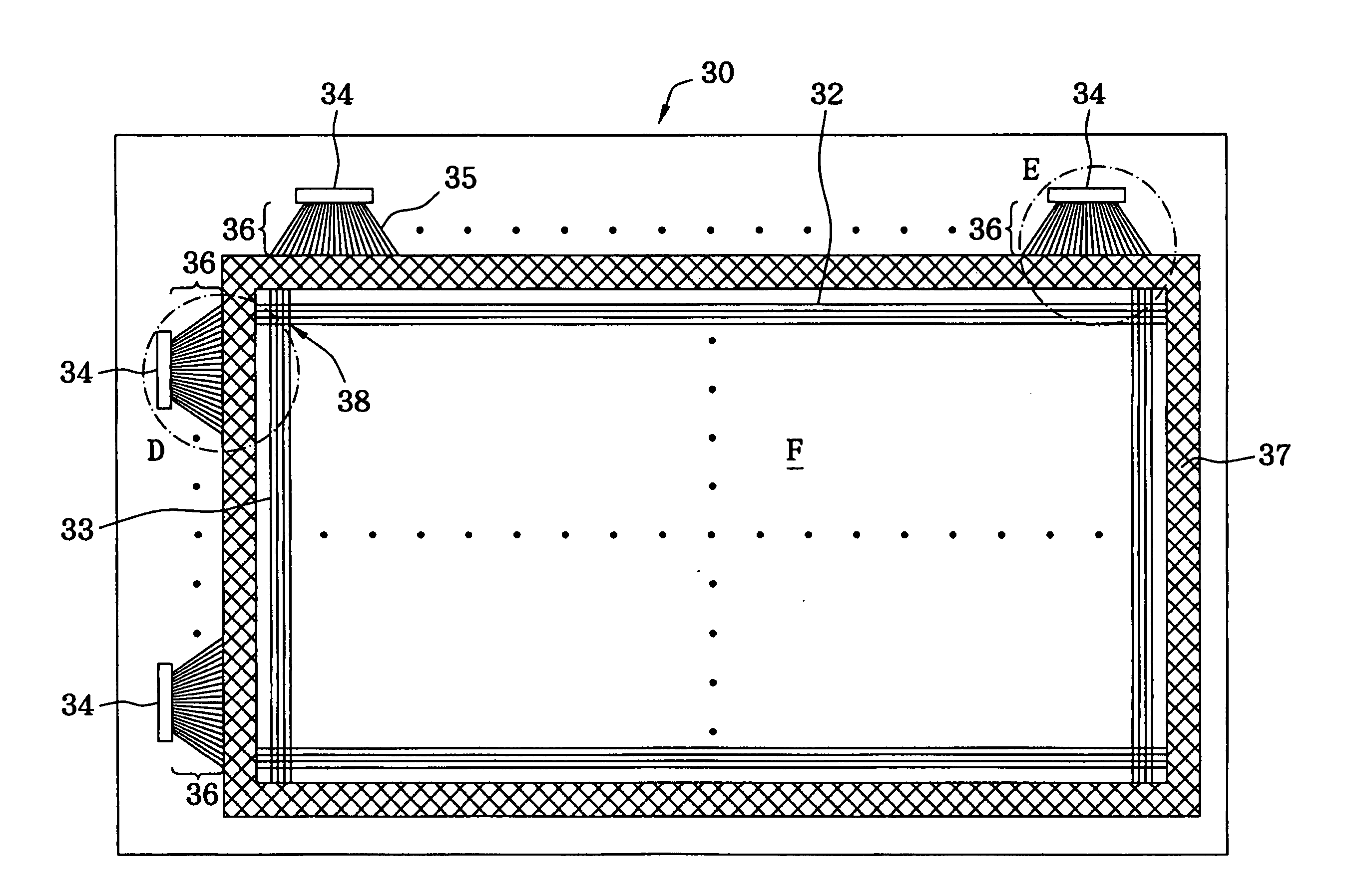
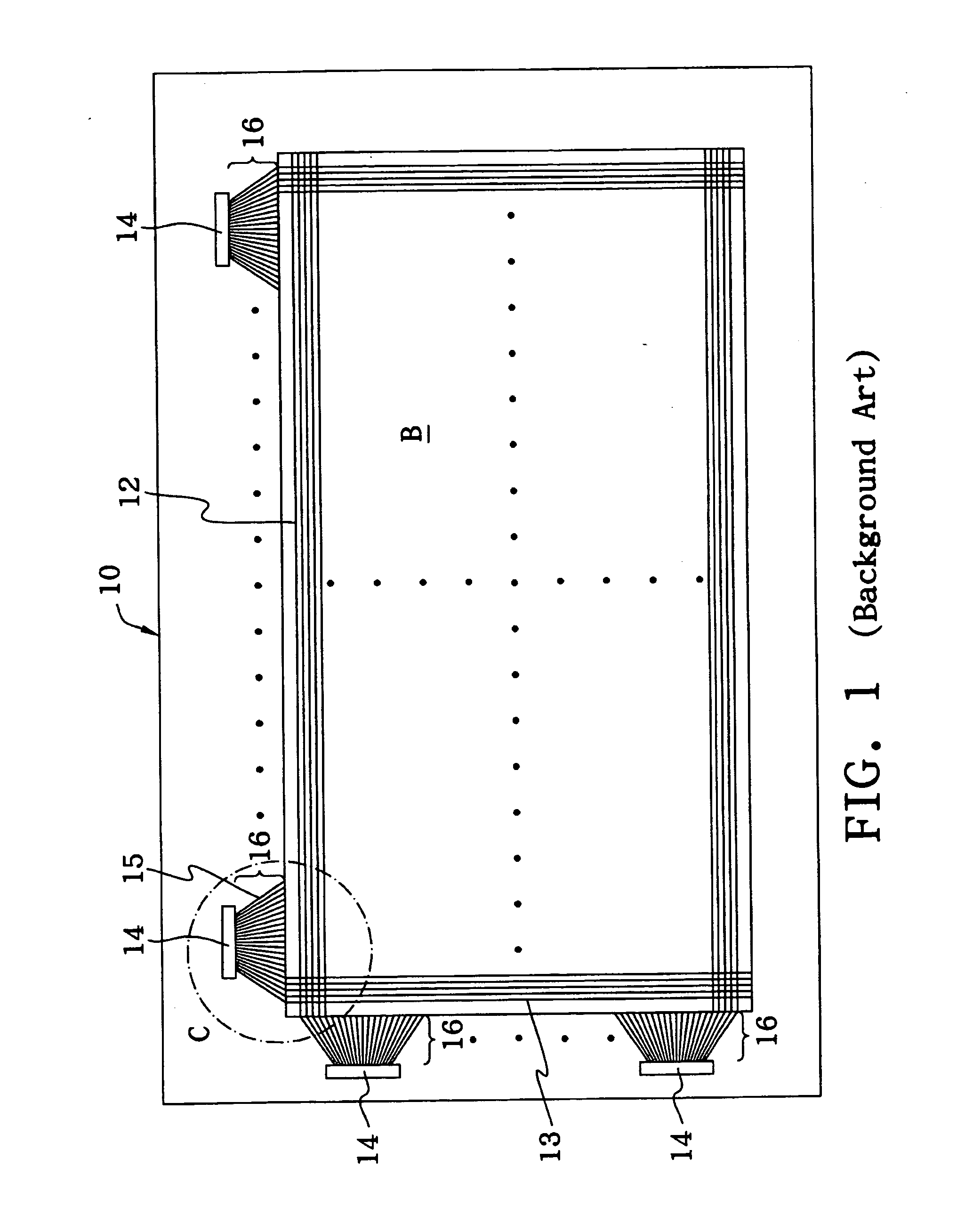
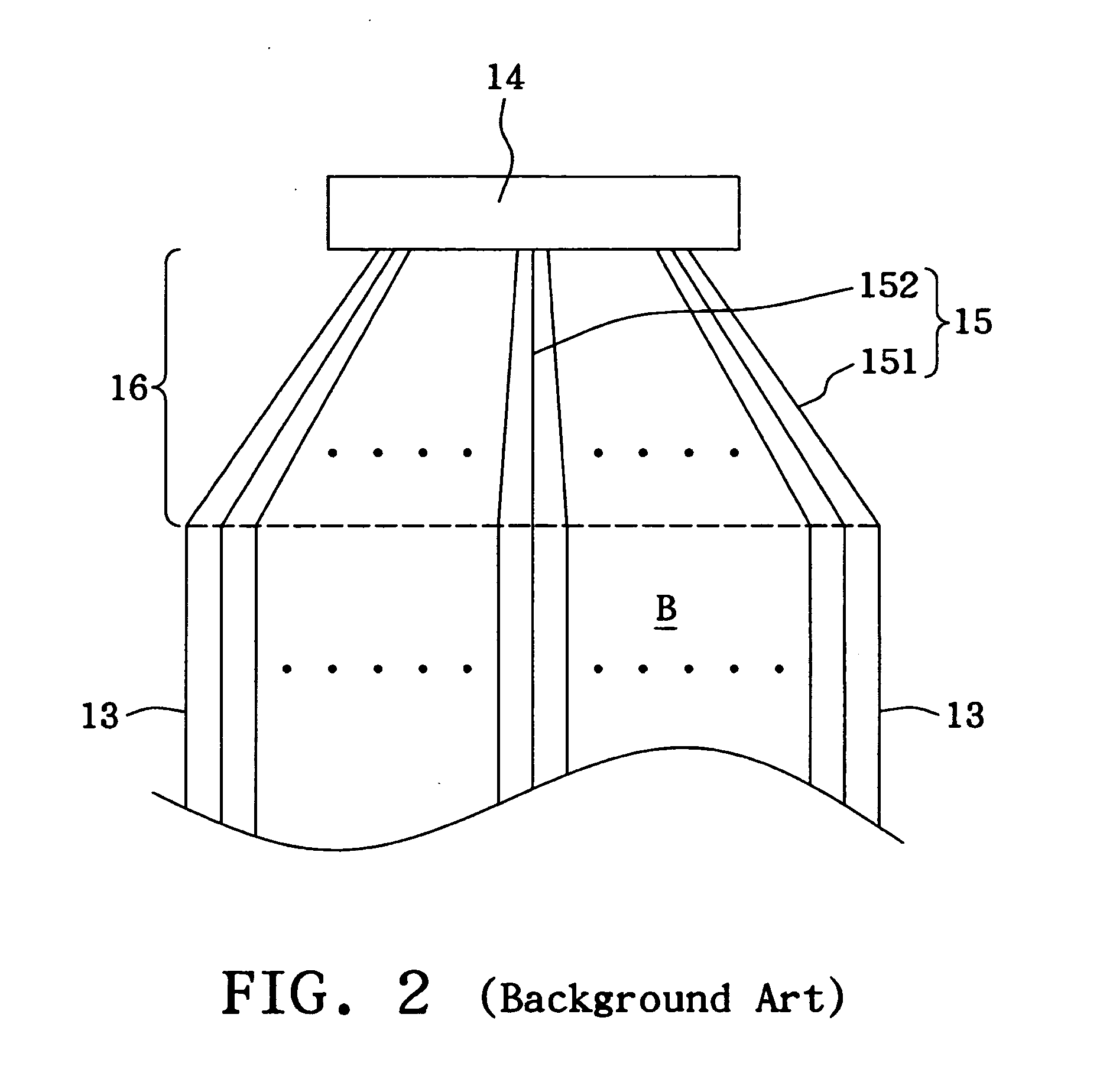
FIG. 3(a) is a circuit layout diagram of an active matrix substrate in accordance with the liquid crystal display panel of the present invention. The active matrix substrate 30 has a plurality of data lines 33 and a plurality of scanning lines 32. The data lines 33 (or named first signal lines) and the scanning lines 32 (or named second signal lines) cross each other to form a plurality of pixels 38 arranged in a matrix, and are all included in signal lines that are responsible to transmit various control signals. In addition, a plurality of thin film transistors (not shown in the figure) are formed within each pixel 38. The total area occupied by the pixels 38 constitutes the active area F.

There are a plurality of outer-lead bonding areas 34 around the active area F. A plurality of pads 341 (as shown in FIG. 4) are formed within the outer lead bonding areas 34, so that driving devices can be connected to the outer lead bonding areas 34 by these pads 341. A fan-out area 36 is dispo...


PUM


Abstract

A liquid crystal display panel with reduced flicker comprises an active matrix substrate equipped with a plurality of thin film transistors. The active matrix substrate has an active area that is formed with a plurality of first signal lines and a plurality of second signal lines crossing each other. The active area includes a plurality of pixels arranged in a matrix. There are outer-lead bonding areas around the active area. There are a plurality of pad areas within the outer-lead bonding areas. A plurality of second wires arranged in a fan-out configuration extend from the pad areas and stretch toward the active area. The second wires are connected to their respective first signal lines by their serpentine or zigzag routes resulting in various wire lengths. A frame-like lead overlaps the second wires, and a capacitor exists between each of the second wires and the closed frame-like lead. The induced capacitor and the resistance of the corresponding second wire together result in a compensation effect so as to uniform the time constants of the plurality of first signal lines.

Description

BACKGROUND OF THE INVENTION 1. Field of the Invention The present invention relates to a liquid crystal display (LCD) panel with reduced flicker and more particularly to a compensation circuit for enabling scanning lines or data lines of the liquid crystal display panel to have the same time constants. 2. Description of the Related Art A conventional liquid crystal display panel comprises an active matrix substrate 10, as shown in FIG. 1. The active matrix substrate 10 has a plurality of data lines 13 and a plurality of scanning lines 12; the data lines 13 and the scanning lines 12 cross each other to form a plurality of pixels arranged in a matrix. In addition, a plurality of thin film transistors (TFTs) are formed within an active area B, which is the area where the data lines 13 and the scanning lines 12 cross perpendicularly. There are a plurality of outer-lead bonding (OLB) areas 14 surrounding the active area B. A plurality of pads are formed within the outer-lead bonding...

Claims


Application Information

Patent Timeline
IPC IPC(8): G02F1/1345
CPCG02F1/1345G09G2320/0223G09G2300/0426G09G3/3611
Inventor JEN, TEAN-SENLIAO, PETERLIN, MING-TIEN
Owner HANNSTAR DISPLAY CORPORATION
Why Eureka
Try Eureka