Method of manufacturing display unit

a display unit and manufacturing method technology, applied in the manufacture of electric discharge tubes/lamps, identification means, instruments, etc., can solve the problems of increasing the number of manufacturing steps, increasing the number of conventional monitors, and increasing the inconvenience of handling and occupied space. , to achieve the effect of high display quality

Inactive Publication Date: 2005-01-27
SONY CORP
View PDF14 Cites 39 Cited by
  • Summary
  • Abstract
  • Description
  • Claims
  • Application Information

AI Technical Summary

Benefits of technology

[0007] The present invention provides a method of manufacturing a display unit capable of manufacturing a large-screen display unit with high display quality without upsizing manufacturing facilities.

Problems solved by technology

However, the larger the scale of a conventional monitor using a CRT (Cathode Ray Tube) or a liquid crystal projector is, the more the weight or the thickness of the conventional monitor increases, so problems such as inconvenience in handling and an increase in occupied space arise.
However, in the conventional method, tiling is performed at first, so the number of manufacturing steps increases.
Moreover, in manufacturing steps after tiling, it is required to upsize all manufacturing facilities, so manufacturing costs pronouncedly increase with renewal of facilities.
Further, in terms of quality, it is difficult to uniformly form an organic layer on a large substrate, thereby it may be difficult to obtain uniform intensity across a screen.

Method used


Image

  • Method of manufacturing display unit
  • Method of manufacturing display unit
  • Method of manufacturing display unit

Examples


Embodiment Construction

[0031] The present invention relates to a method of manufacturing a display unit including a number of small substrates which are aligned so as to upsize the display unit. More specifically, the present invention relates to a method of manufacturing a display unit suitable for manufacturing a large-scale display unit using a top-emitting organic light-emitting device.

[0032] A preferred embodiment of the present invention will be described in more detail below referring to the accompanying drawings.

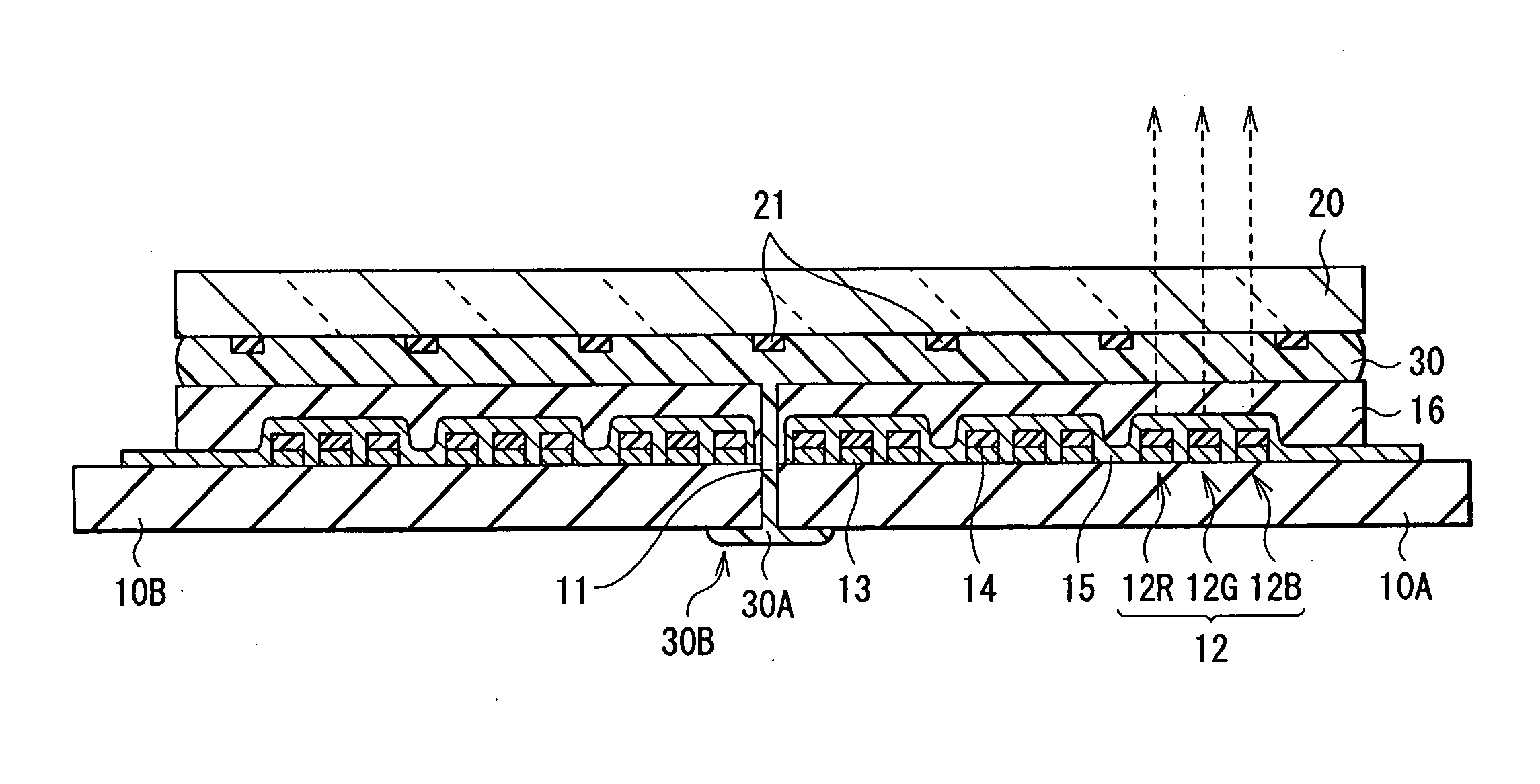
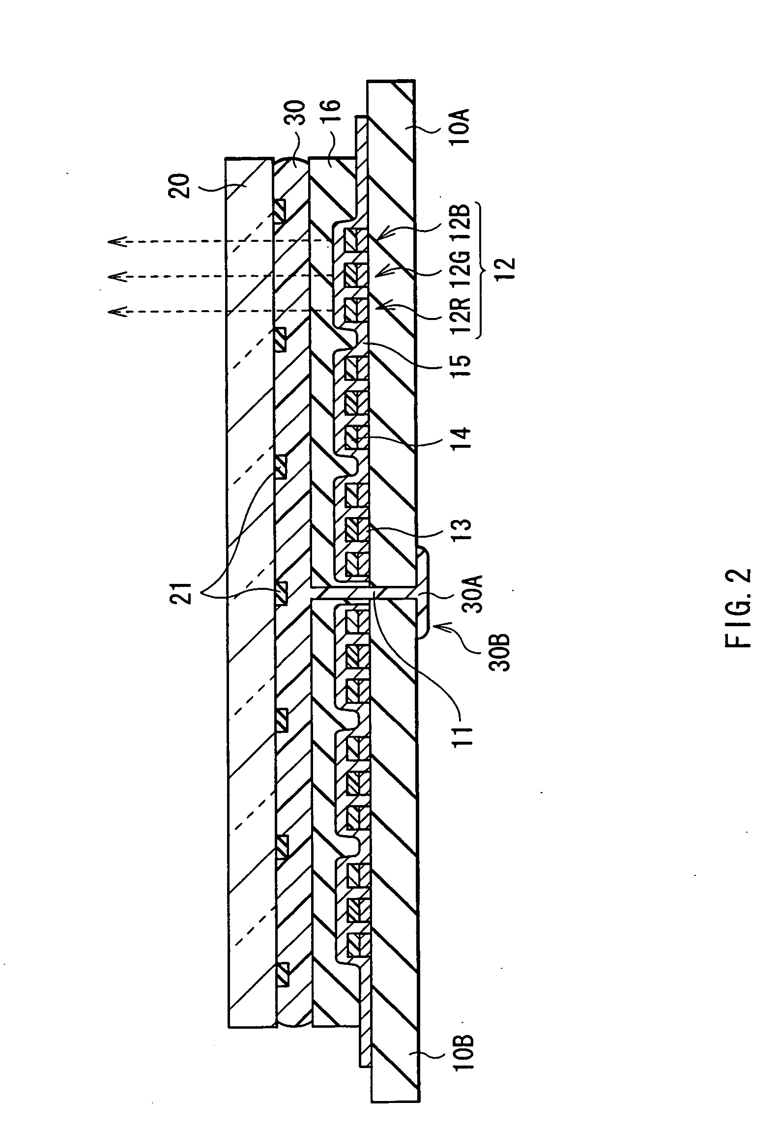
[0033]FIG. 2 shows a sectional view of a display unit according to an embodiment of the invention. The display unit is used as, for example, a medium / large-scale organic light-emitting display unit such as a monitor of a personal computer or a television, or a large-scale organic light-emitting display unit such as a home theater. The display unit has a structure in which a plurality (for example, two) of device substrates 10A and 10B aligned on the same plane and a sealing substrate 20 ...


PUM


Abstract

A method of manufacturing a display unit capable of manufacturing a large-screen display unit with high display quality without upsizing manufacturing facilities is provided. Device substrates on which a pixel including the organic light-emitting devices is formed are aligned on the same plane so as to face a sealing substrate. While the device substrates and the sealing substrate are bonded together with an adhesive resin for sealing in between, the adhesive resin for sealing is extruded from a seam portion to the backside of the seam portion so as to fill the seam portion with the adhesive resin for sealing. The backside of the seam portion can be securely sealed through a simple step. The method is suitable for a large-scale display unit using top-emitting organic light-emitting devices. A back sealing member may be disposed on the backside of the seam portion with the extruded adhesive resin for sealing in between. After that, the adhesive resin for sealing is cured.

Description

CROSS REFERENCES TO RELATED APPLICATIONS [0001] This application claims priority to Japanese Patent Application No. P2003-177887 filed on Jun. 23, 2003, the disclosure of which is incorporated by reference herein. BACKGROUND OF THE INVENTION [0002] The present invention relates to a method of manufacturing a display unit including a number of small substrates which are aligned so as to upsize the display unit. More specifically, the present invention relates to a method of manufacturing a display unit suitable for manufacturing a large-scale display unit using a top-emitting organic light-emitting device. [0003] In recent years, with the rapid advancement of computerization, a need for upsizing of display units such as televisions and monitors has been increasing. The range of uses of large-scale display units is not limited to public places such as railroad stations, airports, lobbies of buildings or hotels and conference rooms, and has been extending to ordinary households. Howeve...

Claims


Application Information

Patent Timeline
Patent Type & Authority Applications(United States)
IPC IPC(8): G09F9/00G09F9/30H05B33/04G09F9/40G09G3/32H01J9/00H01J9/24H01L27/32H01L51/50H01L51/52H05B33/00H05B33/10H05B33/12H05B33/14
CPCG09G2300/0426H01L27/3211H01L51/5284H01L27/3293H01L51/5237H01L27/322H10K59/35H10K59/38H10K59/18H10K50/8426H10K50/844H10K50/865H05B33/10H05B33/04
Inventor TAMASHIRO, HITOSHIIWASE, YUICHITERADA, SHOJI
Owner SONY CORP
Why Eureka
Try Eureka