Electrostatic discharge protection circuit

a protection circuit and electrostatic discharge technology, applied in the direction of semiconductor devices, electrical apparatus, semiconductor/solid-state device details, etc., can solve the problems of permanently disabling circuitry, damage to circuit devices in integrated circuits and other circuitry, permanent disablement of circuitry, etc., and achieve the effect of effectively preventing the damage of devices

Active Publication Date: 2005-02-03
AU OPTRONICS CORP
View PDF1 Cites 22 Cited by
  • Summary
  • Abstract
  • Description
  • Claims
  • Application Information

AI Technical Summary

Benefits of technology

[0009] One object of the present invention is to provide an ESD protection circuit, so that ESD occurring at sp

Problems solved by technology

Electrostatic discharge is a phenomenon that electrostatic charge moves along the surface of a non-conductive material, which might damage circuit devices in an integrated circuit and other circuitry.
During a LCD fabrication, relevant machinery platforms and technicians under operation can carry electrostatic charges, thus when these charge bearers contact the LCD panels, an electrostatic discharge event might take place, and the momentar

Method used


Image

  • Electrostatic discharge protection circuit
  • Electrostatic discharge protection circuit
  • Electrostatic discharge protection circuit

Examples


Embodiment Construction

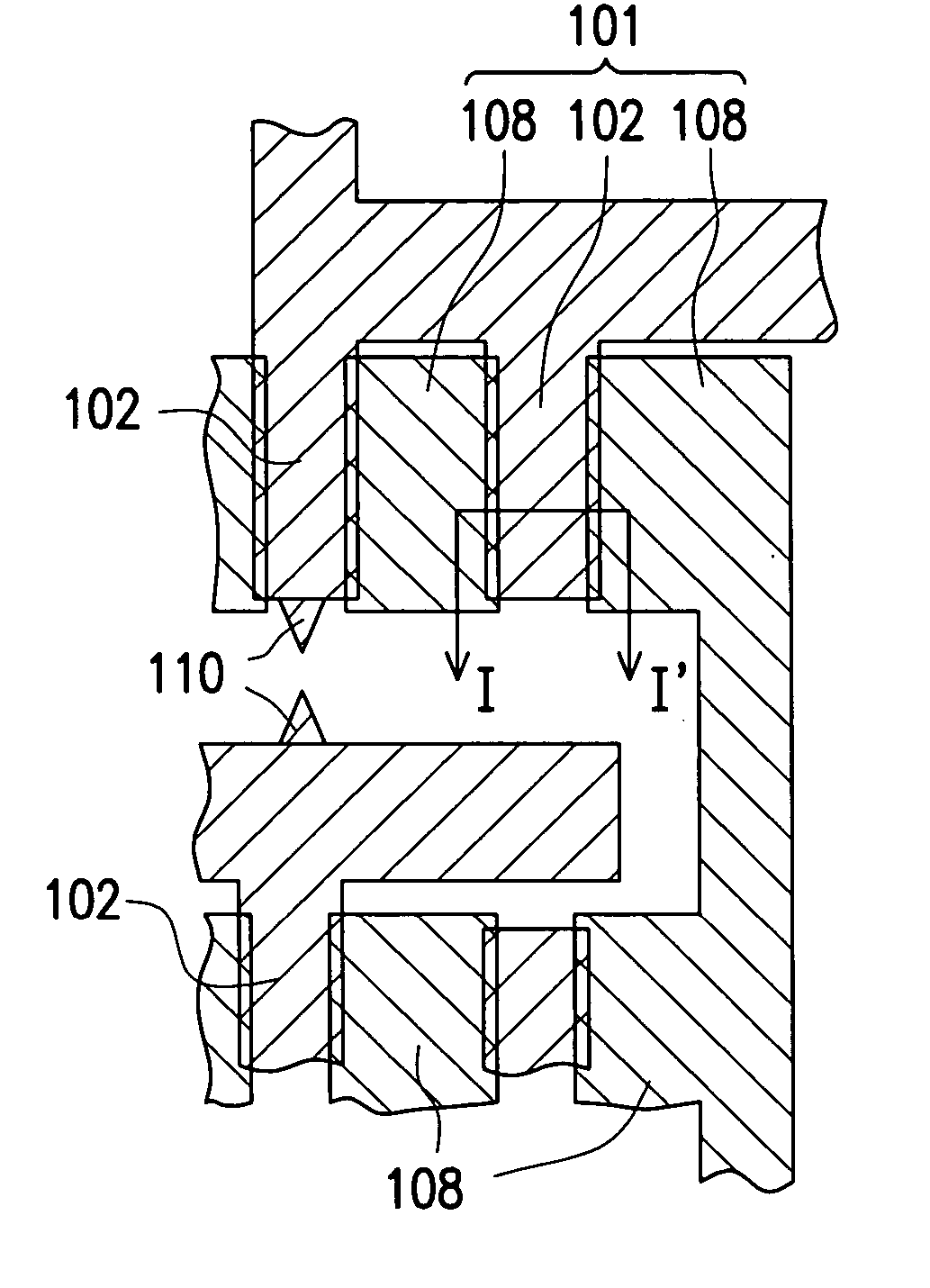
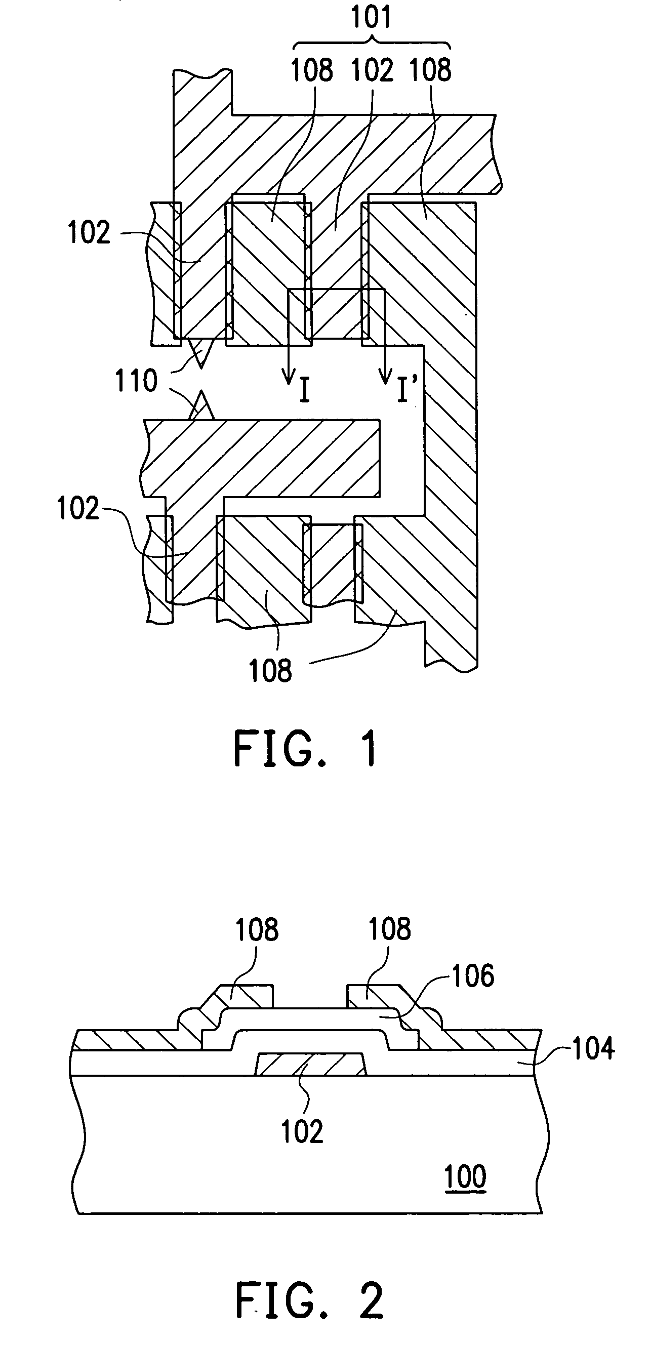
[0027] The present invention provides a structure of an Electrostatic Discharge (ESD) protection circuit having a point structure at prescribed locations, so that electrostatic charges are drained to designated locations. These prescribed locations are designated for avoiding devices or wiring, thus devices and wiring are rendered free from electrostatic impact. In the following paragraphs, a plurality of preferred embodiments is described along with reference to the attached diagrams of the structure of the ESD protection circuit of the present invention. Yet it will be apparent to those skilled in the art that various modifications and variations can be made to the point structure without departing from the spirit and scope of the present invention.

[0028] First Preferred Embodiment

[0029] Referring to FIG. 1, a top view diagram illustrating the structure of the ESD protection circuit according to a first preferred embodiment of the present invention is shown, and FIG. 2 is a cros...


PUM


Abstract

A structure of an electrostatic discharge protection circuit comprises a plurality of thin film transistors and at least a point structure, wherein each of the thin film transistors comprises a gate and a source/drain. The point structure configures at least a portion of a tail or an edge of the gate. In particular, the point structure is located at region apart from the source/drain. The point structures are disposed at prescribed areas apart from devices, and thereby the devices of the electrostatic discharge protection circuit are free from electrostatic discharges.

Description

CROSS-REFERENCE TO RELATED APPLICATION [0001] This application claims the priority benefit of Taiwan application serial no. 92120768, filed on Jul. 30, 2003. BACKGROUND OF THE INVENTION [0002] 1. Field of the Invention [0003] The present invention relates to an electrostatic discharge protection circuit, or ESD protection circuit. More particularly, the present invention relates to an electrostatic discharge protection circuit in a liquid crystal display (LCD). [0004] 2. Description of the Related Art [0005] Electrostatic discharge is a phenomenon that electrostatic charge moves along the surface of a non-conductive material, which might damage circuit devices in an integrated circuit and other circuitry. For instance, when a human being is walking on a carpet, hundreds or even thousands of voltages of electrostatic potential might be detected under high relative humidity, whereas even tens of thousands of voltages might be detected under low relative humidity. [0006] During a LCD f...

Claims


Application Information

Patent Timeline
IPC IPC(8): H01L21/77H01L27/04H01L21/822H01L23/60H01L23/62H01L27/02H01L27/06H01L27/08H01L27/12H01L29/423H01L29/786
CPCH01L27/0251H01L29/42384H01L27/1214H01L27/12H01L27/124
Inventor LAI, HAN-CHUNG
Owner AU OPTRONICS CORP
Why Eureka
Try Eureka