
Display device, a driving method of a display device, and a semiconductor integrated circuit incorporated in a display device

Active Publication Date: 2005-02-03
SEMICON ENERGY LAB CO LTD
View PDF32 Cites 22 Cited by
  • Summary
  • Abstract
  • Description
  • Claims
  • Application Information

AI Technical Summary

Benefits of technology

[0022] Moreover, in the case of the voltage input method adopting the analog gray scale method, a display device is easily affected by variations in TFTs as described above. On the other hand, in the case of the current input method, the writing time of a signal current is lengthened.
[0055] According to the invention, a signal current supplied to a light emitting element can be corrected as the light emitting element varies with time, whereby reducing display variations due to image persistence. Also according to the invention, luminance decay of a light emitting element due to the degradation thereof can be prevented by setting a signal current corresponding to the degradation of the light emitting element, leading to the prevention of lowered image quality.
[0057] Further, according to the invention, a signal current corrected in accordance with the degradation of each light emitting element can be set. Therefore, each light emitting element can be driven more accurately as compared with in the case of correcting a signal current depending on the most degraded light emitting element, and power consumption can be suppressed.

Problems solved by technology

The image persistence causes low quality display in the display device.

Method used


Image

  • Display device, a driving method of a display device, and a semiconductor integrated circuit incorporated in a display device
  • Display device, a driving method of a display device, and a semiconductor integrated circuit incorporated in a display device
  • Display device, a driving method of a display device, and a semiconductor integrated circuit incorporated in a display device

Examples


embodiment

[0119] [Embodiment Mode 3]

[0120] Many methods are possible to correct a signal current in accordance with the degradation of a light emitting element. That is, the invention is characterized in that a current value is corrected depending on the degradation of a light emitting element, and the method of correcting the current value and the like is not exclusively limited.

[0121] In this embodiment mode, shown is a method of correcting a signal current supplied to a light emitting element by using two current sources. Note that in this invention, a single or a plurality of current sources may be employed for correcting a signal current.

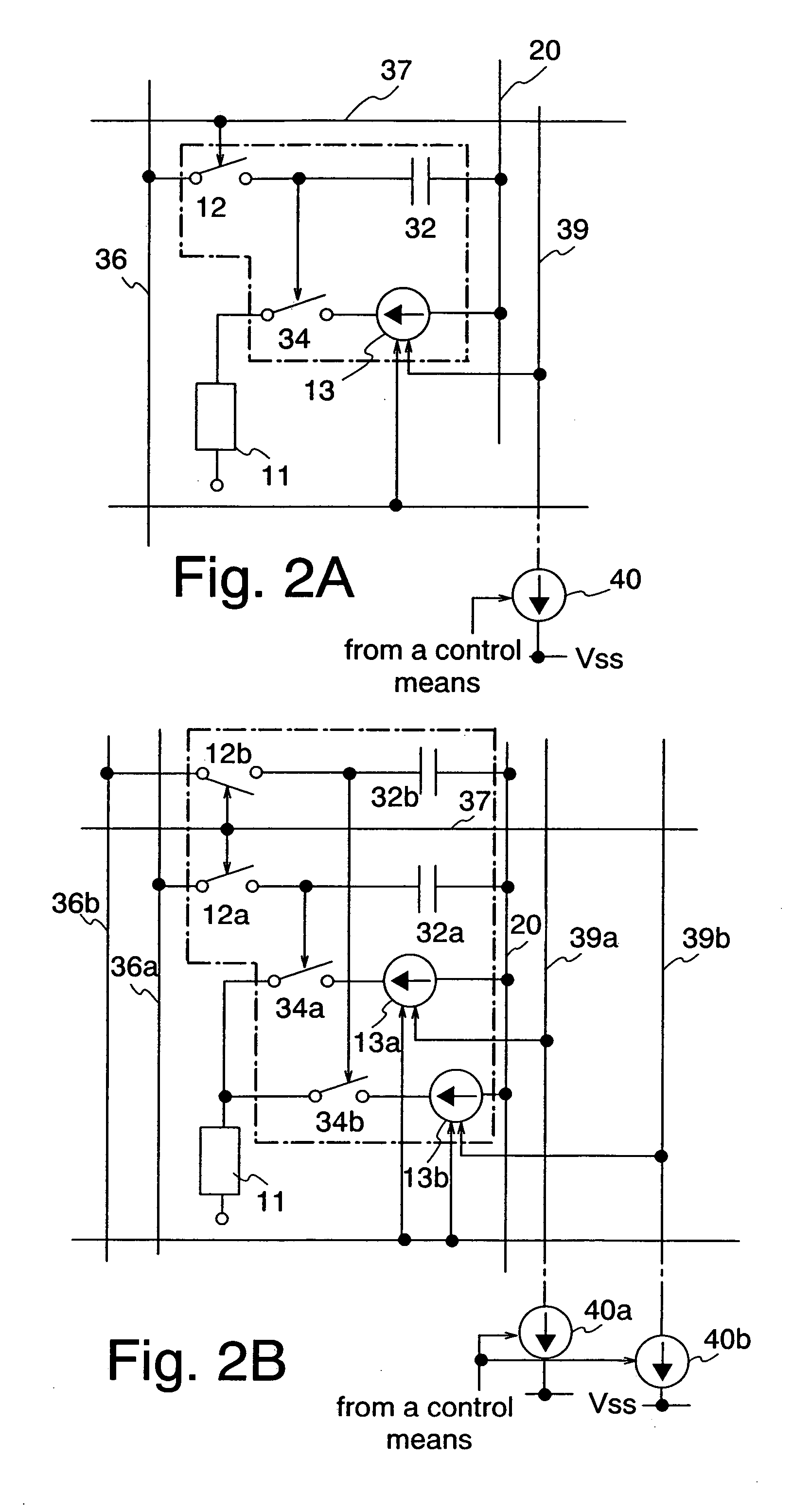
[0122] In FIG. 12A, a first current source 21 and a second current source 22 for setting a corrected signal current are shown. The first current source 21 and the second current source 22 are used as a reference current source and a correction current source respectively. The first and the second current sources 21 and 22 are connected to the same curr...


PUM


Abstract

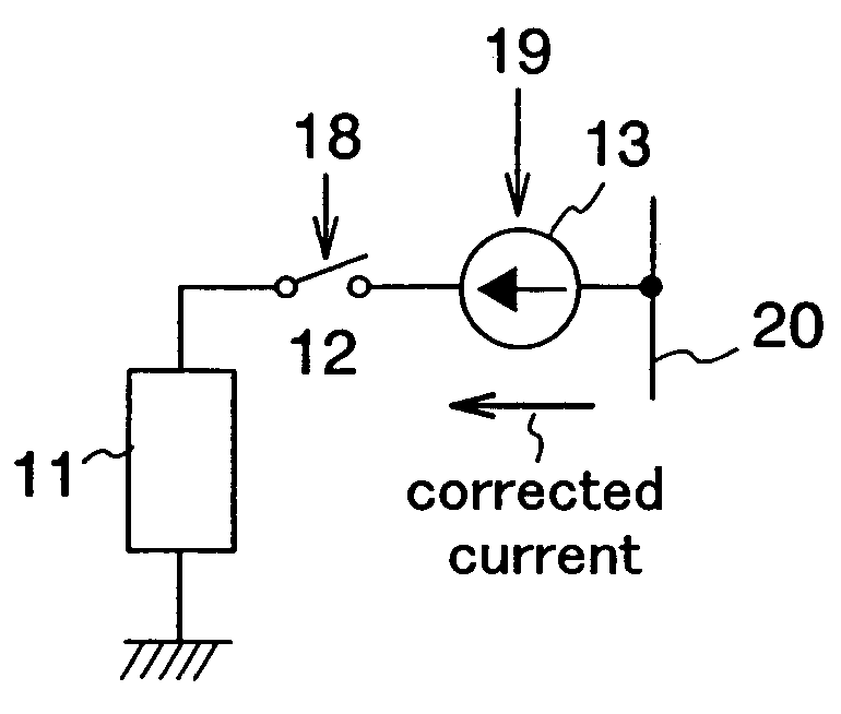
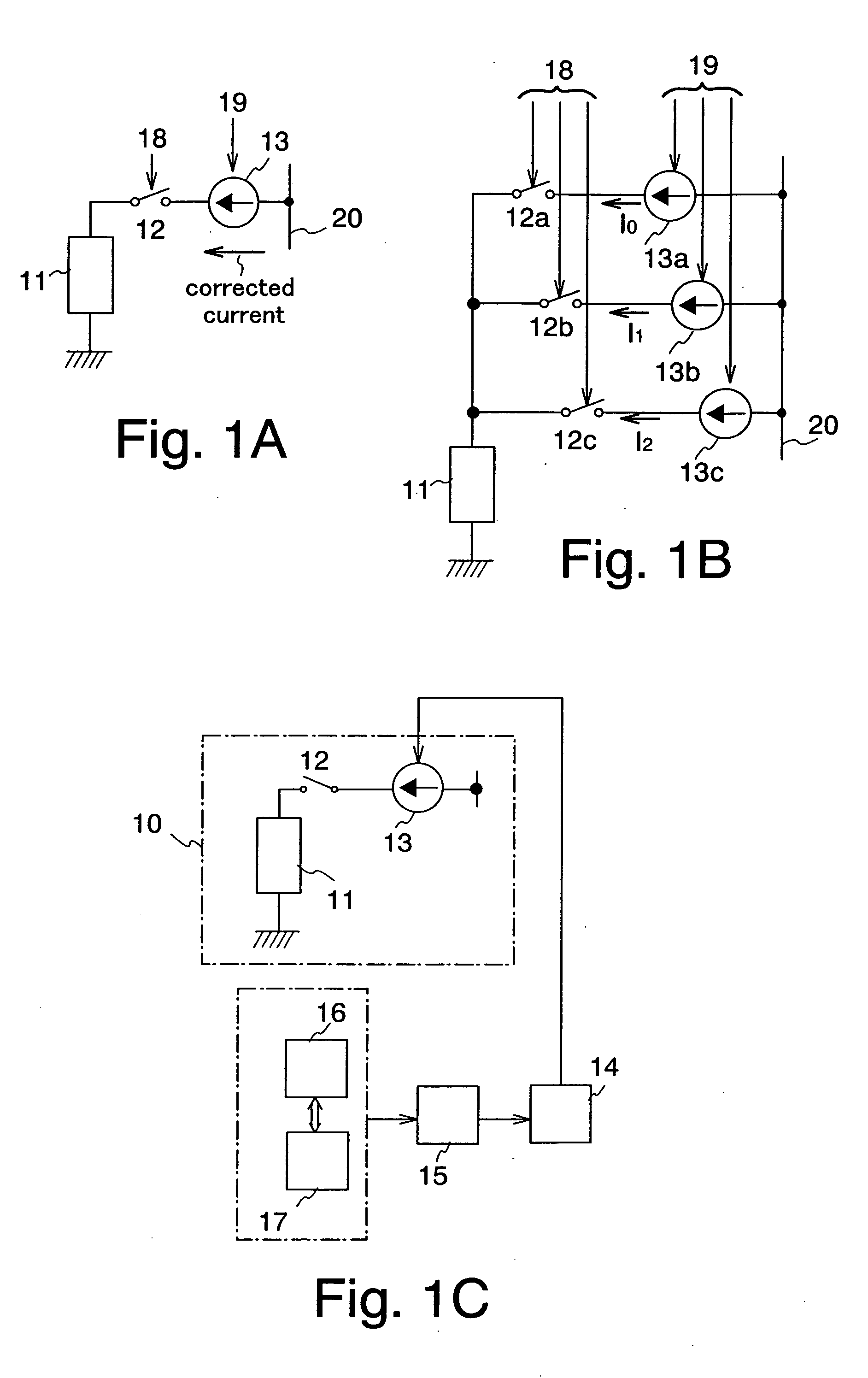
A display device in which a current supplied to a light emitting element is corrected depending on a degradation level of the light emitting element and display variations due to the degradation of each light emitting element are suppressed. Further, according to the display device of the invention, the effect of variations in TFTs is reduced and writing time of a signal is shortened. To achieve the aforementioned display device, according to the invention, a current value supplied to a light emitting element is corrected in accordance with the degradation thereof instead of correcting a video signal. Further, the display device comprises at least a supply source for supplying a corrected current depending on the degradation of a light emitting element and a current source for supplying the corrected current from the supply source to the light emitting element. Moreover, according to such a display device, a first current source of the supply source supplies a corrected current corresponding to the degradation of the least degraded light emitting element of the light emitting elements connected to the same signal line, meanwhile a second current source supplies a corrected current corresponding to the degradation of the most degraded light emitting element of the light emitting elements connected to the same signal line.

Description

BACKGROUND OF THE INVENTION [0001] 1. Field of the Invention [0002] The present invention relates to a display device, particularly an active matrix display device having self-light emitting elements, and to a driving method of a display device. The invention further relates to a semiconductor integrated circuit incorporated in a display device. [0003] 2. Description of the Related Art [0004] In recent years, a display device using a light emitting element (self-light emitting element) has been studied and developed. Such a display device has the advantages of high image quality, reduced thickness, light weight or the like, and thus it is widely used as a screen of a mobile phone and a monitor of a personal computer. In particular, since the light emitting display device has the features such as low voltage drive, low power consumption, and fast response which contributes to dynamic display, it is expected to be used for various electronic apparatuses typified by a next-generation m...

Claims


Application Information

Patent Timeline
IPC IPC(8): G09F9/30G09G3/20G09G3/30G09G3/32H05B33/14H05B44/00
CPCG09G3/3233G09G3/3291G09G2300/0819G09G2300/0842G09G2320/048G09G2300/0861G09G2320/0252G09G2320/043G09G2300/0852
Inventor KIMURA, HAJIMEKOYAMA, JUN
Owner SEMICON ENERGY LAB CO LTD
Learn More