Semiconductor processor control systems, semiconductor processor systems, and systems configured to provide a semiconductor workpiece process fluid

a technology of semiconductor workpieces and control systems, applied in the direction of grinding machine components, manufacturing tools, lapping machines, etc., can solve the problems of stray particles produced by polishing and adverse effects of polishing

Inactive Publication Date: 2005-02-03
MOORE SCOTT E +2
View PDF48 Cites 33 Cited by
  • Summary
  • Abstract
  • Description
  • Claims
  • Application Information

AI Technical Summary

Benefits of technology

[0011] According to certain aspects of the present invention, a control system is configured to monitor a process fluid within a semiconductor processor system. The control system is configured to control operations of the semiconductor processor system responsive to such monitoring of the process fluid.
[0012] One aspect of the present invention provides a mixing system configured to mix plural components to form a process fluid. The disclosed control system is configured to monitor and control such mixing operations. The semiconductor processor system also provides a sampling system according to other aspects of the invention. The sampling system is configured to draw and monitor samples of a process fluid. Another aspect of the invention provides a flush system and recirculation system configured to respectively flush and recirculate fluid within an associated connection of the semiconductor processor system. Additional aspects of the invention provide monitoring of a connection for accumulation of particulate matter. The disclosed control system monitors such accumulation and implements responsive operations.

Problems solved by technology

Furthermore, polishing can produce stray particles from the semiconductor wafer, pad material or elsewhere.
Polishing may be adversely affected once these by-products reach a sufficient concentration.

Method used


Image

  • Semiconductor processor control systems, semiconductor processor systems, and systems configured to provide a semiconductor workpiece process fluid
  • Semiconductor processor control systems, semiconductor processor systems, and systems configured to provide a semiconductor workpiece process fluid
  • Semiconductor processor control systems, semiconductor processor systems, and systems configured to provide a semiconductor workpiece process fluid

Examples


Embodiment Construction

[0044] This disclosure of the invention is submitted in furtherance of the constitutional purposes of the U.S. Patent Laws “to promote the progress of science and useful arts” (Article 1, Section 8).

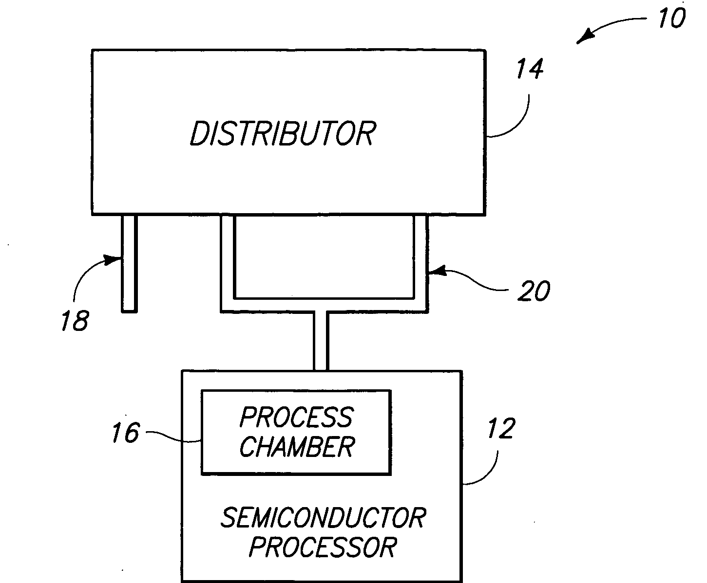
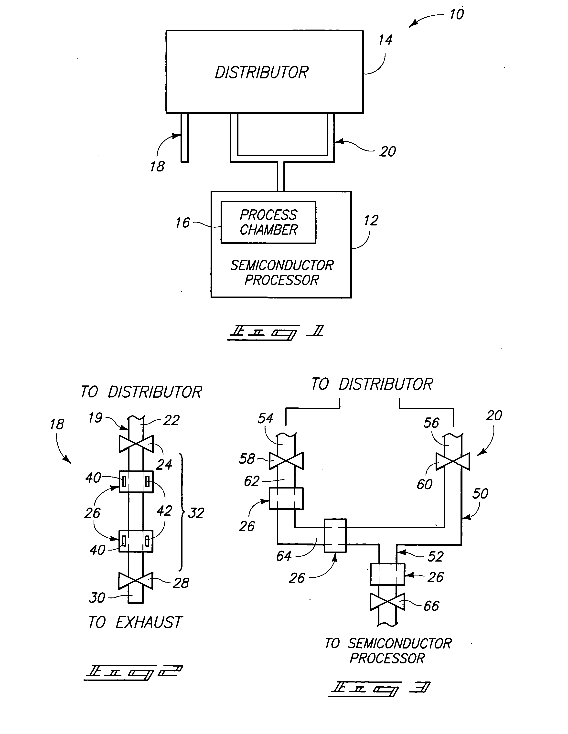
[0045] Referring to FIG. 1, a semiconductor processing system 10 is illustrated. The depicted semiconductor processing system 10 includes a semiconductor processor 12 coupled with a distributor 14. Semiconductor processor 12 includes a process chamber 16 configured to receive a semiconductor workpiece, such as a silicon wafer. In an exemplary configuration, semiconductor processor 12 is implemented as a chemical-mechanical polishing processing tool.

[0046] Distributor 14 is configured to supply a subject material for use in semiconductor workpiece processing operations. For example, distributor 14 can supply a subject material comprising a slurry to semiconductor processor 12 for chemical-mechanical polishing applications.

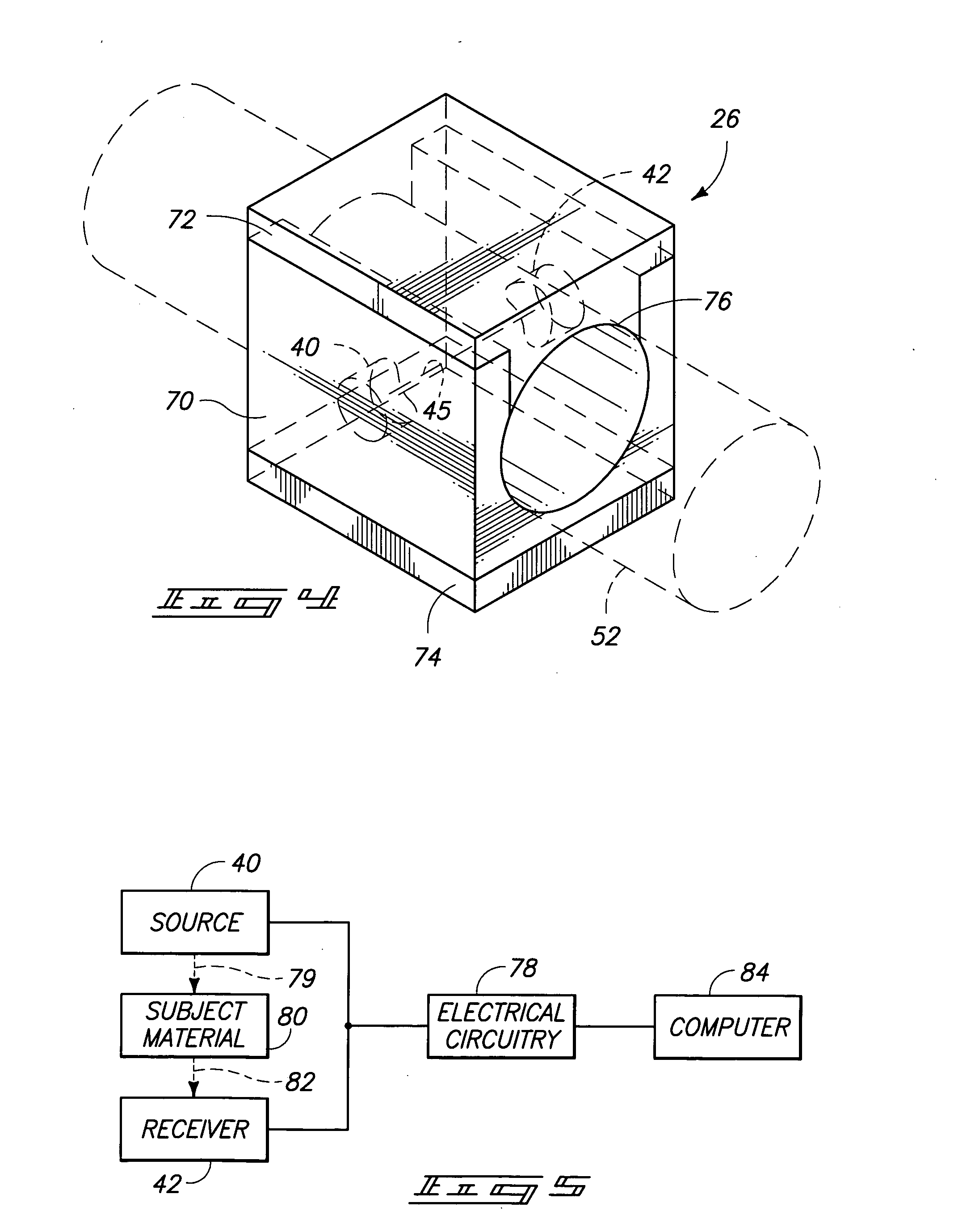
[0047] Exemplary conduits or piping of semiconductor processing ...


PUM


Abstract

Semiconductor processor systems, systems configured to provide a semiconductor workpiece process fluid, semiconductor workpiece processing methods, methods of preparing semiconductor workpiece process fluid, and methods of delivering semiconductor workpiece process fluid to a semiconductor processor are provided. One aspect of the invention provides a semiconductor processor system including a process chamber adapted to process at least one semiconductor workpiece using a process fluid; a connection coupled with the process chamber and configured to receive the process fluid; a sensor coupled with the connection and configured to output a signal indicative of the process fluid; and a control system coupled with the sensor and configured to control at least one operation of the semiconductor processor system responsive to the signal.

Description

RELATED PATENT DATA [0001] The present application is a continuation-in-part of patent application Ser. No. 09 / 324,737 which was filed on Jun. 3, 1999 and which is incorporated by reference herein.TECHNICAL FIELD [0002] The present invention relates to semiconductor processor systems, systems configured to provide a semiconductor workpiece process fluid, semiconductor workpiece processing methods, methods of preparing semiconductor workpiece process fluid, and methods of delivering semiconductor workpiece process fluid to a semiconductor processor. BACKGROUND OF THE INVENTION [0003] Numerous semiconductor processing tools are typically utilized during the fabrication of semiconductor devices. One such common semiconductor processor is a chemical-mechanical polishing (CMP) processor. A chemical-mechanical polishing processor is typically used to polish or planarize the front face or device side of a semiconductor wafer. Numerous polishing steps utilizing the chemical-mechanical polis...

Claims


Application Information

Patent Timeline
Patent Type & Authority Applications(United States)
IPC IPC(8): B24B37/04B24B49/10B24B57/02
CPCB24B37/04B24B57/02B24B49/10
Inventor MOORE, SCOTT E.MEIKLE, SCOTT G.CRUM, MAGDEL
Owner MOORE SCOTT E
Why Eureka
Try Eureka