Semiconductor light emitting device

a technology of semiconductor light and light-emitting devices, which is applied in the direction of semiconductor light-emitting devices, basic electric elements, electrical appliances, etc., can solve the problems of increasing the power consumption per unit amount of electric current of the semiconductor light-emitting devices, and achieve the effect of small power consumption

Active Publication Date: 2005-02-10
ROHM CO LTD
View PDF2 Cites 31 Cited by
  • Summary
  • Abstract
  • Description
  • Claims
  • Application Information

AI Technical Summary

Benefits of technology

[0009] The present invention, in order to solve the above-described problems, has an object to provide a semiconductor light emitting device that enables making small the power consumption and enables uniformly causing light to be emitted in a light emitting portion included in the light emitting portion formative layer.

Problems solved by technology

However, if the multilayered reflection layer 61 that is located at a stage that is lower from the cathode electrode 56 is made to come near to the active layer 54 and thereby the distance between the multilayered reflection layer 61 and the cathode electrode 56 shortens, the resistance value near the cathode electrode 56 becomes high with the result that the power consumption per unit amount of electric current of the semiconductor light emitting device increases.

Method used


Image

  • Semiconductor light emitting device
  • Semiconductor light emitting device
  • Semiconductor light emitting device

Examples


Embodiment Construction

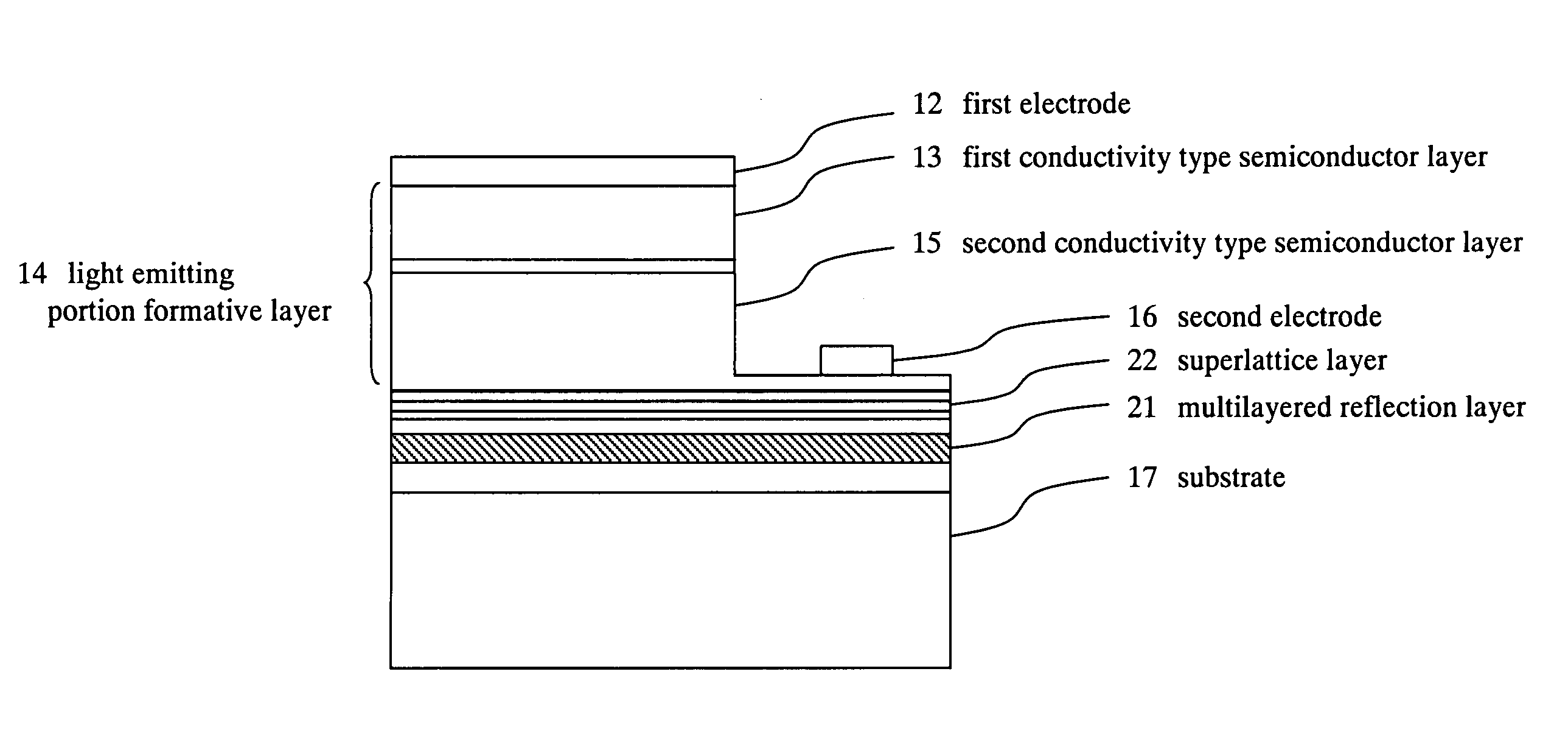
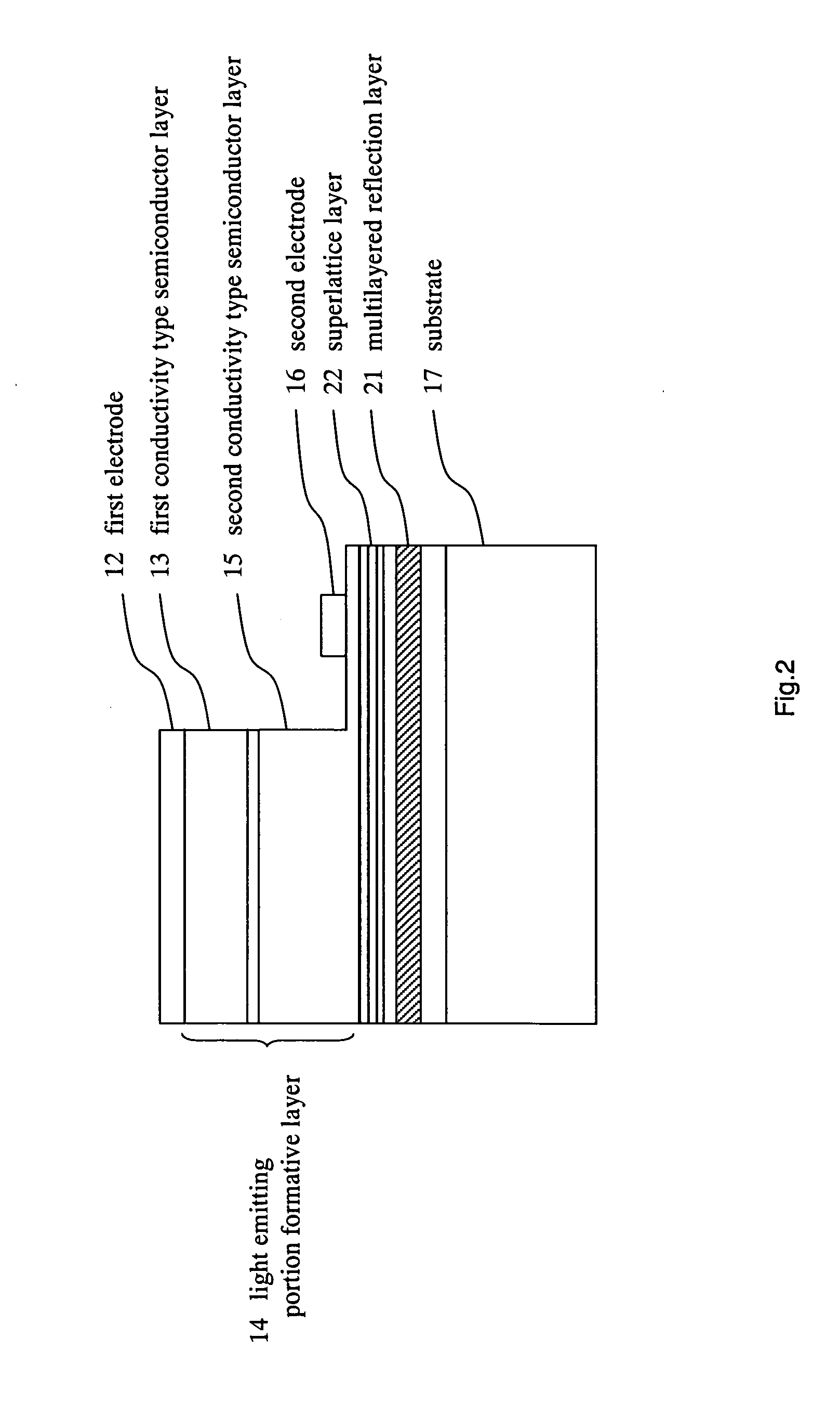
[0016] Hereinafter, an embodiment of the invention of this application will be explained using FIGS. 2 and 3. FIGS. 2 and 3 are views illustrating examples of the embodiment of the invention of this application. In FIGS. 2 and 3, a reference numeral 12 denotes a first electrode, a reference numeral 13 denotes a first conductivity type semiconductor layer, a reference numeral 15 denotes a second conductivity type semiconductor layer, a reference numeral 14 denotes a light emitting portion formative layer, a reference numeral 16 denotes a second electrode, a reference numeral 17 denotes a substrate, a reference numeral 21 denotes a multilayered reflection layer, and a reference numeral 22 denotes a superlattice layer. It is to be noted that this embodiment is only illustrative of the invention of this application and the invention of this application permits various changes and modifications to be made without impairing the subject matter of the invention, and the invention of this ap...


PUM


Abstract

In a III group nitride compound semiconductor wherein light that has been emitted in a light emitting portion formative layer is reflected by a multilayered reflection layer that is provided between the light emitting portion formative layer and sapphire substrate, it is desirable, for increasing the reflection efficiency of the light that has been emitted in the light emitting portion formative layer, that the multilayered reflection layer be provided at a position that is as near to the light emitting portion as possible. However, since the multilayered reflection layer is high in resistance value and also high in power consumption, locating the multilayered reflection layer near the light emitting portion formative layer results in that the resistance value in the vicinity of a relevant cathode electrode becomes increased. This raises the problem that emission of light occurs only in part of the light emitting portion formative layer. In the semiconductor light emitting device of the present invention, a superlattice layer is provided between the light emitting portion formative layer and the cathode electrode.

Description

BACKGROUND OF THE INVENTION [0001] 1. Field of the Invention [0002] The disclosure of Japanese Patent Application No. 2003-206217 filed Aug. 6, 2003 including specification, drawings and claims is incorporated herein by reference in its entirety. [0003] The present invention relates to a semiconductor light emitting device that is comprised of a III group nitride compound semiconductor. More particularly, the invention concerns a semiconductor light emitting device comprised of a compound semiconductor, which is equipped with a multilayered reflection layer and a superlattice layer. [0004] 2. Description of the Related Art [0005] In FIG. 1, there is illustrated a conventional semiconductor light emitting device that is comprised of a III group nitride compound semiconductor. In FIG. 1, a reference numeral 57 denotes a sapphire substrate, a reference numeral 55 denotes an n-type semiconductor layer, a reference numeral 61 denotes a multilayered reflection layer, a reference numeral 5...

Claims


Application Information

Patent Timeline
Patent Type & Authority Applications(United States)
IPC IPC(8): H01L27/15H01L33/06H01L33/10H01L33/32
CPCH01L33/04H01L33/32H01L33/10
Inventor ISHIKAWA, TSUTOMU
Owner ROHM CO LTD
Why Eureka
Try Eureka