Electronic substrate, semiconductor device, and electronic device

Inactive Publication Date: 2007-09-06
SEIKO EPSON CORP
View PDF6 Cites 43 Cited by
  • Summary
  • Abstract
  • Description
  • Claims
  • Application Information

AI Technical Summary

Benefits of technology

[0037]According to this configuration, electronic device includes the electronic substrate in which the tra

Problems solved by technology

However, when a connection terminal is formed on the electronic substrate, there are problems in that the structure becomes complex, or the packaging operation of the connection terminal on other electronic substrate or motherboard becomes complex and troublesome.

Method used


Image

  • Electronic substrate, semiconductor device, and electronic device
  • Electronic substrate, semiconductor device, and electronic device
  • Electronic substrate, semiconductor device, and electronic device

Examples


first embodiment

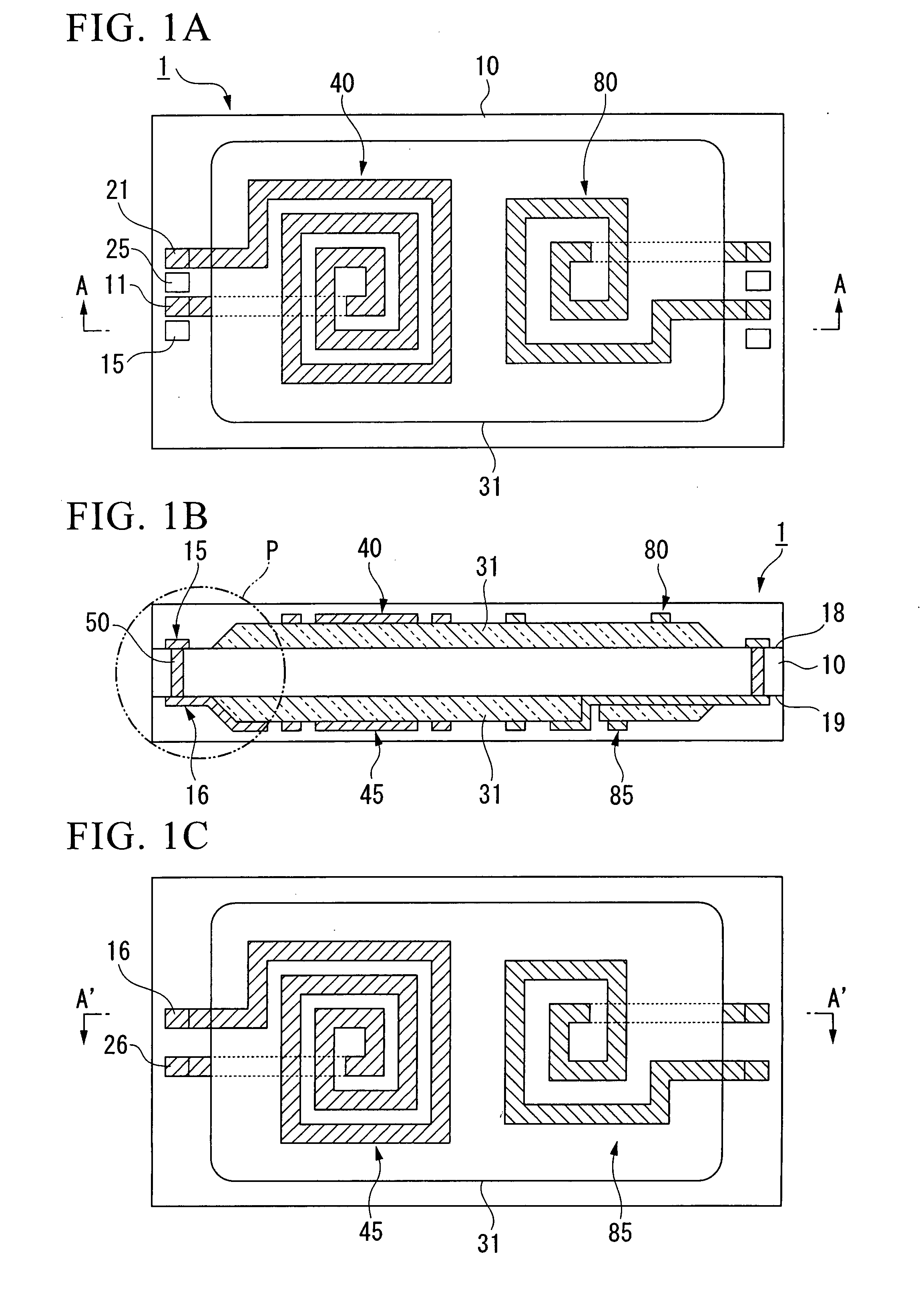
[0050]The electronic substrate related to the first embodiment is described here at first.

[0051]FIGS. 1A to 1C are explanatory views of the electronic substrate related to the first embodiment. FIG. 1A shows a plan view, FIG. 1C shows a bottom view, and FIG. 1B shows a cross-sectional view taken along the line A-A in FIG. 1A (cross-sectional view taken along the line A′-A′ in FIG. 1C).

[0052]As shown in FIG. 1B, electronic substrate 1 related to the first embodiment includes a base substrate 10 made of a material such as silicon, glass, quartz, or crystal, and a plurality of inductor elements 40, 45, 80, and 85.

[0053]The inductor elements 40, 80 are each formed with different inductance value or different applicable frequency on the active face 18 of the base substrate 10.

[0054]The inductor elements 45 and 85 are each formed with different inductance value or different applicable frequency on the rear face 19 of the base substrate 10.

[0055]Electronic circuit (not shown in the figures...

second embodiment

[0174]Next, the electronic substrate related to the second embodiment is described here.

[0175]FIGS. 6A and 6B are explanatory views of the electronic substrate related to the second embodiment. FIG. 6A shows a plan view, while FIG. 6B shows the cross-sectional view taken along the line F-F in FIG. 6A.

[0176]As shown in FIG. 6A, electronic substrate 1 related to the second embodiment differs from the first embodiment that performs power transmission using inductor elements in that it performs power transmission using connection terminal 63.

[0177]Moreover, the electronic substrate related to the second embodiment differs from the first embodiment in that it performs communications using a plurality of inductor elements 80 and 90.

[0178]Note that detailed explanations of parts with the same configuration as the first embodiment are omitted here.

[0179]Relocated Wiring and So On

[0180]As shown in FIG. 6A, a plurality of electrodes 62 are aligned along the peripheral edge of electronic subst...


PUM


Abstract

An electronic substrate includes: a base substrate having an active face and a rear face; inductor elements formed on or above the active face, and formed on or above the rear face; and a conductive member electrically connected to the inductor element formed on or above the rear face, penetrating through the base substrate from the active face to the rear face.

Description

CROSS-REFERENCE TO RELATED APPLICATION[0001]This application claims priority from Japanese Patent Application No. 2006-057673, filed Mar. 3, 2006, the contents of which are incorporated herein by reference.BACKGROUND[0002]1. Technical Field[0003]The present invention relates to electronic substrate, semiconductor device, and electronic device.[0004]2. Related Art[0005]Electronic substrates (semiconductor chips) with integrated circuits are provided in electronic devices such as mobile telephones, notebook personal computers, and personal data assistants (PDA).[0006]Generally, a connection terminal is formed in the electronic substrate, which is packaged on other electronic substrate or motherboard through this connection terminal.[0007]This allows signals such as power transmission signals and communication signals to be exchanged between the electronic substrate and other electronic substrate or motherboard.[0008]However, when a connection terminal is formed on the electronic subst...

Claims


Application Information

Patent Timeline
IPC IPC(8): H01F5/00
CPCH01F5/003H01F17/0006H01F17/0013H01F27/292H01L2224/16H01Q1/2266H01Q1/2283H01Q1/38H01F38/14H01L23/12
Inventor HASHIMOTO, NOBUAKI
Owner SEIKO EPSON CORP
Why Eureka
Try Eureka