Method for separating semiconductor wafer from supporting member, and apparatus using the same

a technology of semiconductor wafers and supporting components, applied in the direction of transportation and packaging, layered products, other domestic articles, etc., can solve the problems of brittle thin semiconductor wafers, easy distortion, and difficult handling and achieve the effect of smooth separation of thin semiconductor wafers

Inactive Publication Date: 2005-02-10
NITTO DENKO CORP
View PDF4 Cites 28 Cited by
  • Summary
  • Abstract
  • Description
  • Claims
  • Application Information

AI Technical Summary

Benefits of technology

[0011] The present invention is made in view of the above circumstances and its object is to provide a method and apparatus for separating a semiconductor wafer from a supporting member, capable of smoothly separating the semiconductor wafer integrally with a dicing frame from the supporting member without stress.

Problems solved by technology

Such a thin semiconductor wafer is brittle and easily distorted and its handling is extremely difficult.
In the case where a both-faced adhesive sheet has heating separability such that the sheet foams when being heated and its adhesive strength disappears, if a semiconductor wafer is restrained by being sandwiched by upper and lower two tables, foaming (expansion) of the both-faced adhesive sheet is disturbed and the adhesive strength cannot be sufficiently reduced.
As a result, a problem occurs such that the semiconductor wafer cannot be smoothly separated from the supporting member.
For example, when the both-faced adhesive sheet whose adhesive strength has not disappeared is separated together with the supporting member from the semiconductor wafer, there is a possibility in that local separation stress acts on the semiconductor wafer and a warp or breakage may occur.
There is also a problem that an adhesive remains on the surface of semiconductor wafer.

Method used


Image

  • Method for separating semiconductor wafer from supporting member, and apparatus using the same
  • Method for separating semiconductor wafer from supporting member, and apparatus using the same
  • Method for separating semiconductor wafer from supporting member, and apparatus using the same

Examples


first embodiment

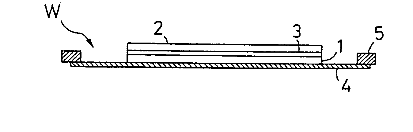
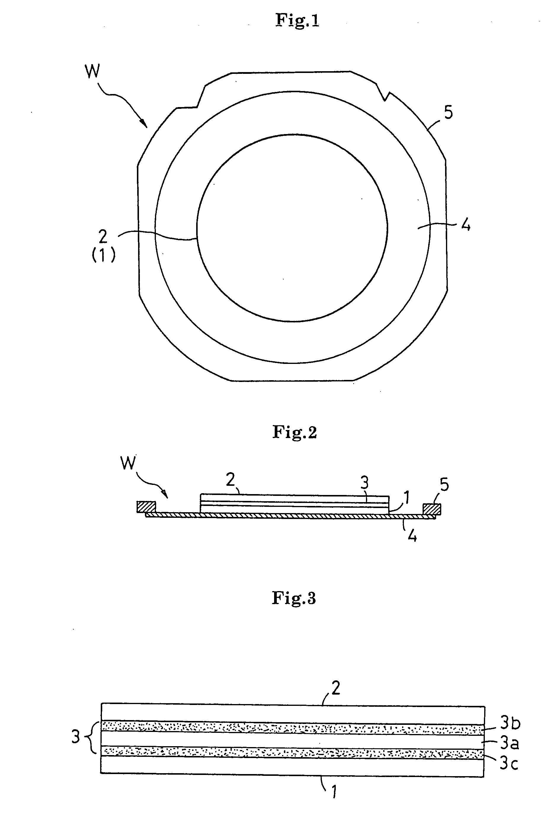
[0071]FIG. 1 is a plan view of a work W obtained by joining and fixing a semiconductor wafer 1 to which a supporting member 2 taking the form of a glass plate is joined via a both-faced adhesive sheet to a dicing frame 5 via a dicing tape 4. FIG. 2 is a vertical cross sectional view of the work W. FIG. 3 is a side view of the semiconductor wafer 1 to which the supporting member 2 is joined via a both-faced adhesive sheet 3.

[0072] As shown in FIG. 2, the supporting member 2 is joined to a device formation face (surface) of the semiconductor wafer 1 via the both-faced adhesive sheet 3. In a state where the back face of the semiconductor wafer 1 is backing-reinforced by the supporting member 2, the back face of the semiconductor wafer 1 is ground to a desired thickness in a back grinding process. After that, the semiconductor wafer 1 is joined and fixed to the ring-shaped dicing frame 5 via the dicing tape 4, and loaded into a dicing apparatus.

[0073] Herein, the both-faced adhesive s...

second embodiment

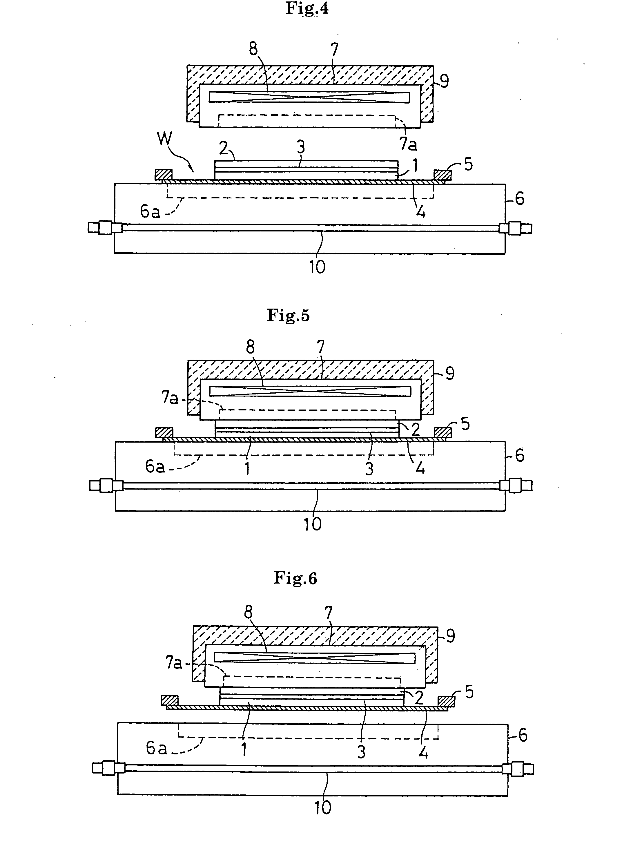
[0085] In a second embodiment, a case where both ends of the dicing frame 5 are mounted on the top ends of lower holding members such as plate materials, transport belts, or the like will be described as an example.

[0086]FIG. 9 is a plan view showing a state where a work is mounted and held, and FIGS. 10 to 13 are side views each illustrating a separating process performed by separating means.

[0087] As shown in FIG. 9, a work W is loaded so that both ends of the dicing frame 5 are mounted on the top ends of lower holding members 11 such as plate materials, transport belts, or the like. A cooling stage 12 is disposed between the lower holding members 11. The lower holding member 11 corresponds to first holding means of the present invention, and the cooling stage 12 corresponds to cooling means.

[0088] A cooling device 13 is buried in the cooling stage 12, and a cooling air injection part 14 is provided on the top face of the cooling stage 12. By blowing cooling air to the under fa...


PUM

PropertyMeasurementUnit
thicknessaaaaaaaaaa
adhesive strengthaaaaaaaaaa
thicknessaaaaaaaaaa

Abstract

A work is suction-held by an upper suction chuck stage from the surface side of a supporting member, is moved upward to a predetermined height, and is heated in a state where the thickness direction of a both-faced adhesive sheet is not restricted, and a dicing tape is cooled. After lapse of predetermined heating time, the work is separated from the both-faced adhesive sheet whose adhesive strength is weaken, and drops to a lower suction chuck stage.

Description

BACKGROUND OF THE INVENTION [0001] (1) Field of the Invention [0002] The present invention relates to a semiconductor wafer separating method for joining a dicing tape to a semiconductor wafer to which a supporting member is joined via a double-faced adhesive sheet, fixing the resultant to a dicing frame, and separating the semiconductor wafer integrally with the dicing frame from the supporting member, and to a separating apparatus used for the method. [0003] (2) Description of the Related Art [0004] In resent years, with rapid progress of an application, reduction in thickness of a semiconductor wafer to 100 μm to 50 μm, in some occasions, even to 25 μm is demanded. Such a thin semiconductor wafer is brittle and easily distorted and its handling is extremely difficult. Consequently, the semiconductor wafer is held by being joined to the surface side of a supporting member having strength such as a glass plate via a both-faced adhesive sheet. After the semiconductor wafer is reinfo...

Claims


Application Information

Patent Timeline
Patent Type & Authority Applications(United States)
IPC IPC(8): B32B43/00H01L21/67B65H41/00H01L21/00H01L21/30H01L21/301H01L21/304H01L21/68H01L21/78
CPCB32B43/006B32B2457/14H01L21/67109H01L21/67132H01L2221/6834H01L21/6836H01L2221/68318H01L2221/68327H01L21/6835H01L21/68
Inventor MIYAMOTO, SABUROHASE, YUKITOSHI
Owner NITTO DENKO CORP
Why Eureka
Try Eureka