Integrated device with an improved BIST circuit for executing a structured test

a structured test and integrated device technology, applied in digital circuit testing, electronic circuit testing, instruments, etc., can solve the problems of poor fault coverage, high cost of external test equipment, and poor structure performan

Active Publication Date: 2005-02-10
STMICROELECTRONICS SRL
View PDF22 Cites 21 Cited by
  • Summary
  • Abstract
  • Description
  • Claims
  • Application Information

AI Technical Summary

Problems solved by technology

The main disadvantage of the solutions known in the art is the use of external test equipment for applying the input test vectors or the seeds to the integrated device and for comparing the output test vectors with the expected test data.
Furthermore, it is necessary to carefully synchronize the external test equipment with a system clock of the integrated device for detecting transition faults in the functional circuitry; therefore, when the frequency of operation of the integrated device is high, the external test equipment becomes very expensive.
However, this structure provides poor performance in terms of fault coverage.

Method used


Image

  • Integrated device with an improved BIST circuit for executing a structured test
  • Integrated device with an improved BIST circuit for executing a structured test
  • Integrated device with an improved BIST circuit for executing a structured test

Examples


Embodiment Construction

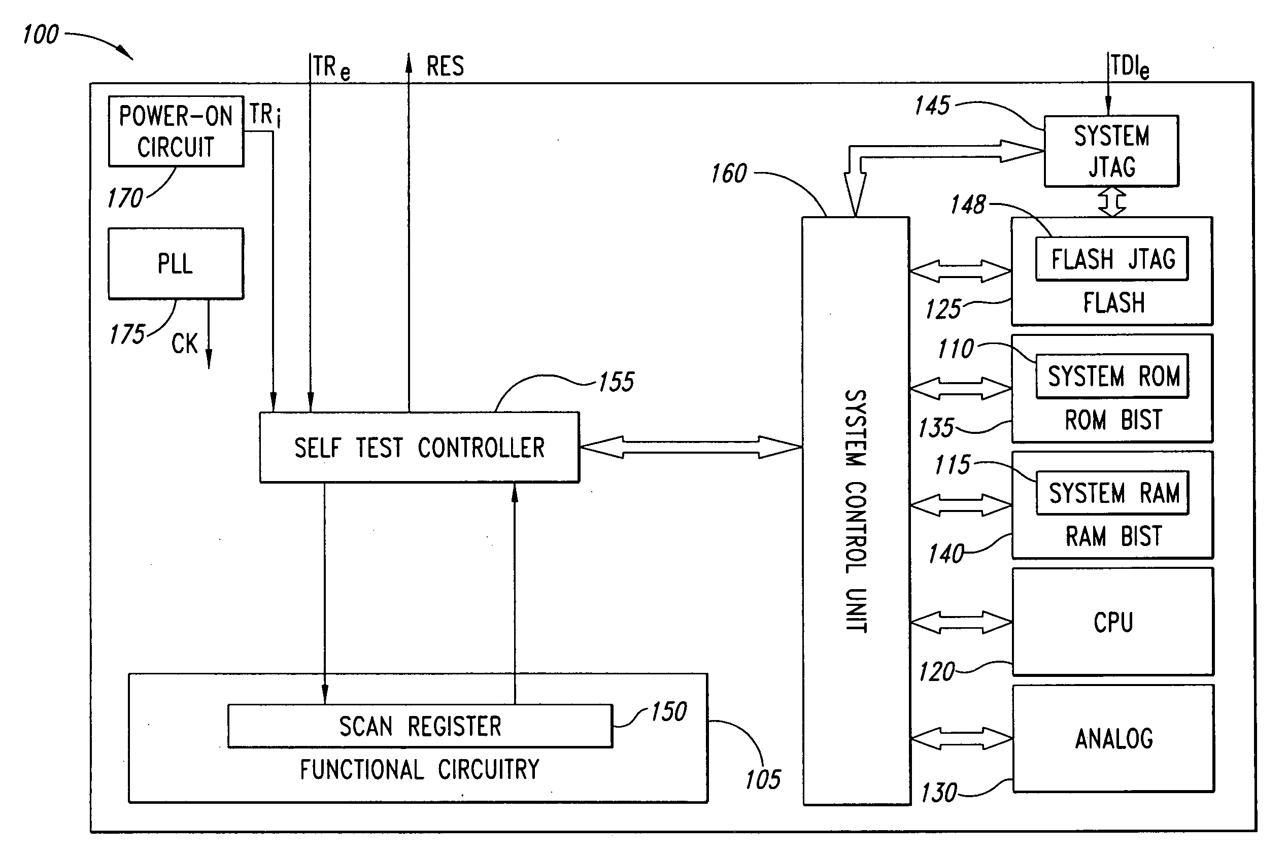
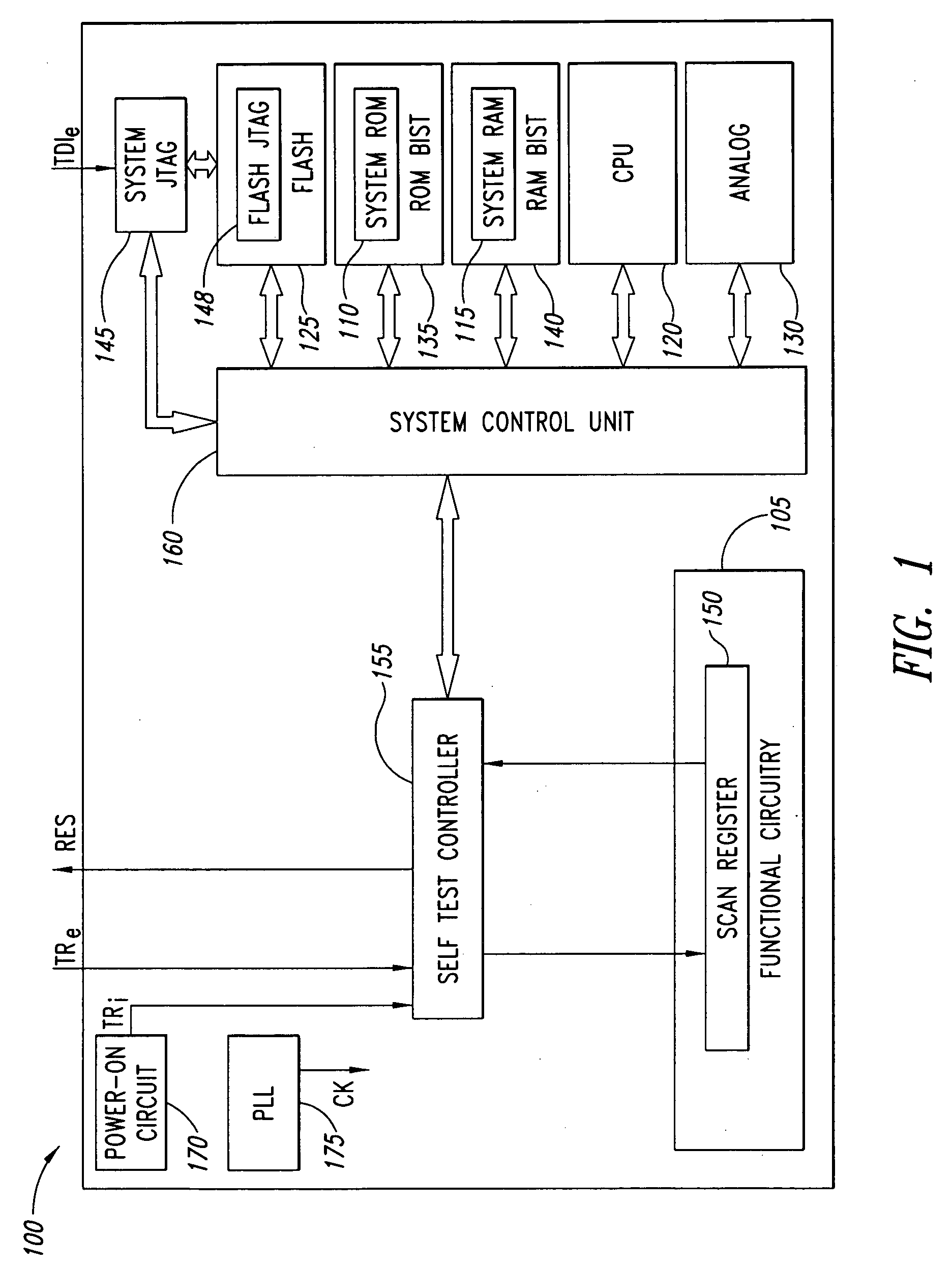
[0017] With reference in particular to FIG. 1, a schematic block diagram of an integrated device 100, in which the solution of the invention is applicable, is shown. For example, the integrated device 100 consists of a System on Chip; particularly, the integrated device 100 includes a functional circuitry 105, a system ROM memory 110, a system RAM memory 115, a CPU 120 (i.e., a central processing unit), a system flash memory 125 and an analog circuitry 130.

[0018] The system ROM memory 110 and the system RAM memory 115 are included in a system ROM BIST circuit 135 and in a system RAM BIST circuit 140, respectively. A test on the system ROM and RAM memories 110, 115 and on the system flash memory 125 is allowed by a JTAG interface 145, compatible with the IEEE standard 1149.1; the JTAG interface 145 receives an external test signal TDIe, and is coupled with a corresponding interface 148 of the system flash memory 125.

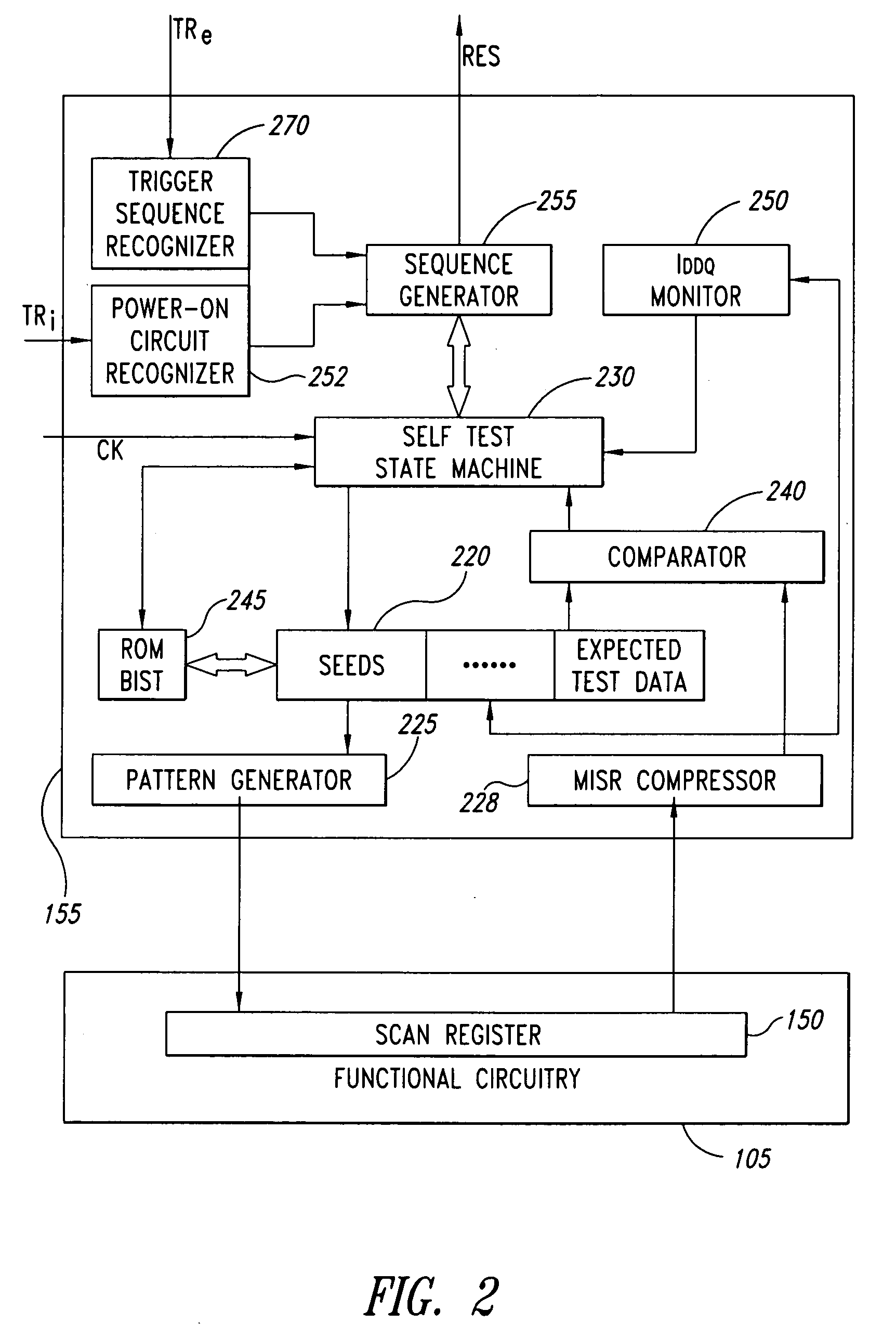
[0019] A self test controller 155 is embedded in the integrated de...


PUM


Abstract

An integrated device including a functional circuitry and a built-in self testing circuit for executing a structured test on the functional circuitry is proposed. The functional circuitry includes means for receiving input test values from the built-in self testing circuit and returning output test values to the built-in self testing circuit. In the solution of the invention, the built-in self testing circuit includes a memory for storing starting test values and expected test values, means for generating the input test values according to the starting test values, and means for determining a result of the structured test according to a comparison between the output test values and the expected test values.

Description

BACKGROUND OF THE INVENTION [0001] 1. Field of the Invention [0002] The present invention relates to an integrated device with a Built-in Self Testing (BIST) circuit for executing a structured test. [0003] 2. Description of the Related Art [0004] The structured test is a technique that has become increasingly popular in the last years, especially for testing complex integrated circuits. For this purpose, the integrated device is provided with internal structures permitting the controllability and the observability of each pin and / or internal sequential element (referred to as a node). [0005] A known and commonly used technique for executing the structured test is the scan method. In this method, the integrated device is provided with boundary scan cells (for the pins) and / or internal scan cells (for the internal nodes). The boundary scan cells are serially connected in a chain and the internal scan cells are serially connected in one or more chains (between corresponding input pins ...

Claims


Application Information

Patent Timeline
Patent Type & Authority Applications(United States)
IPC IPC(8): G01R31/00G01R31/30G01R31/317G01R31/3185G01R31/3187
CPCG01R31/006G01R31/3004G01R31/3187G01R31/318547G01R31/318577G01R31/31724
Inventor CASARSA, MARCO
Owner STMICROELECTRONICS SRL
Why Eureka
Try Eureka