Method of dividing a plate-like workpiece

Active Publication Date: 2005-02-17
DISCO CORP
View PDF3 Cites 21 Cited by
  • Summary
  • Abstract
  • Description
  • Claims
  • Application Information

AI Technical Summary

Benefits of technology

[0013] According to the present invention, since the non-processed area is left behind in at least one end portion of each dividing line and grooves are not formed in this area in the laser beam application step, the cutting blade can carry out stable cutting in

Problems solved by technology

As the Low-k film consists of multi-layers (5 to 15 layers) like mica and is extremely fragile, when the semiconductor wafer having the above Low-k film laminated thereon is cut along a dividing line with a cutting blade, a problem occurs that the Low-k film peels off, and this peeling reaches a circuit and gives a fatal damage to

Method used


Image

  • Method of dividing a plate-like workpiece
  • Method of dividing a plate-like workpiece
  • Method of dividing a plate-like workpiece

Examples


Embodiment Construction

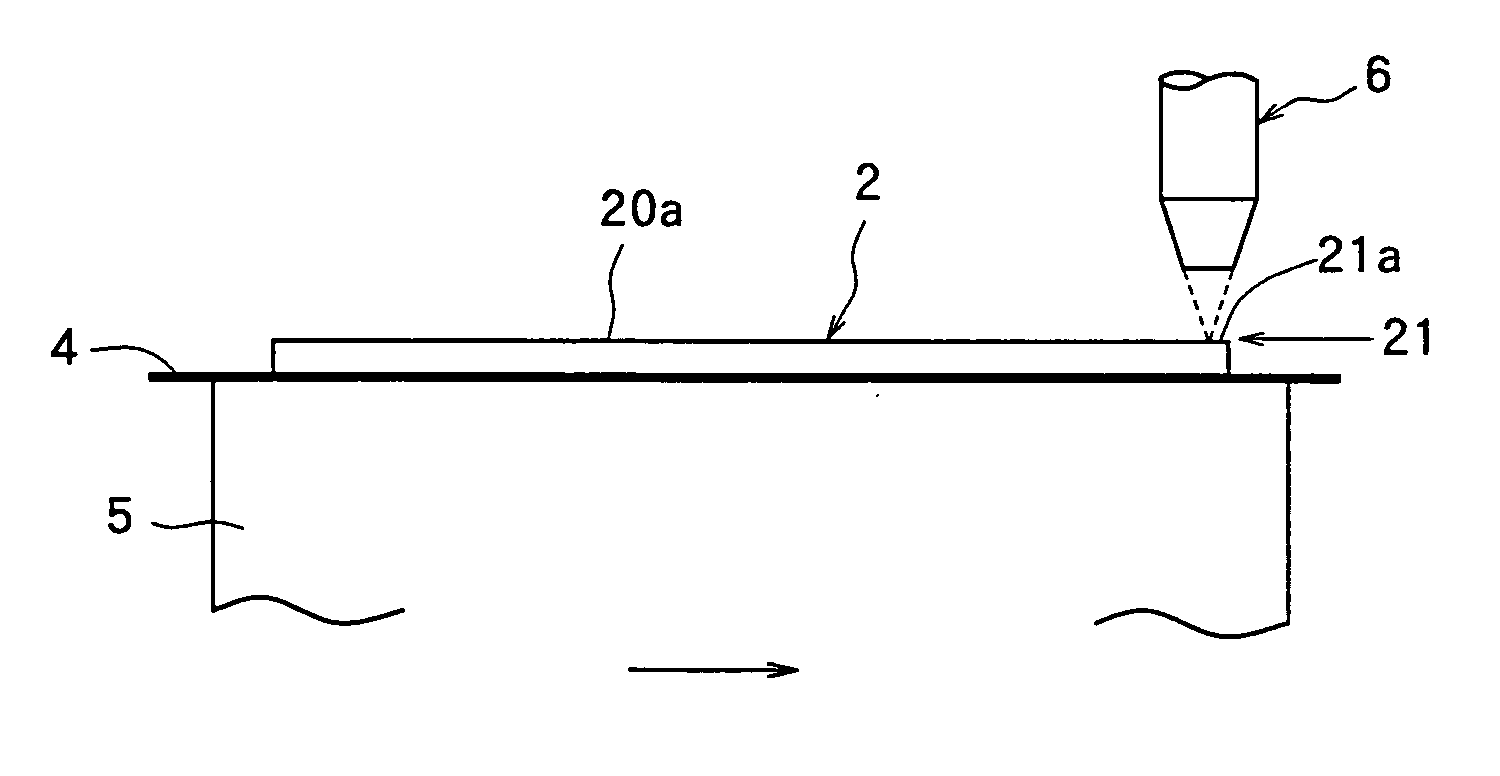
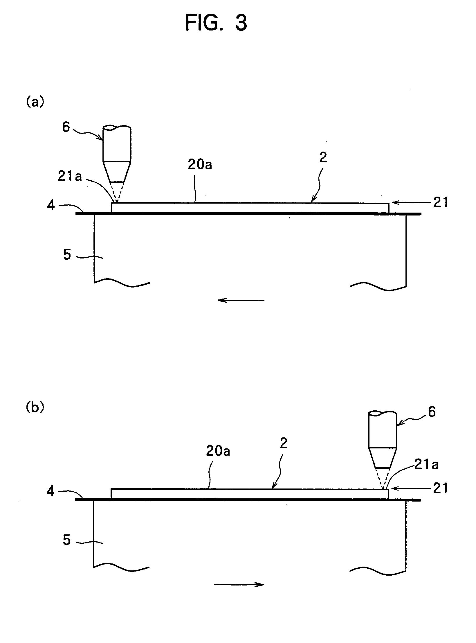
[0023] The method of dividing a plate-like workpiece according to the present invention will be described in more detail hereinafter with reference to the accompanying drawings.

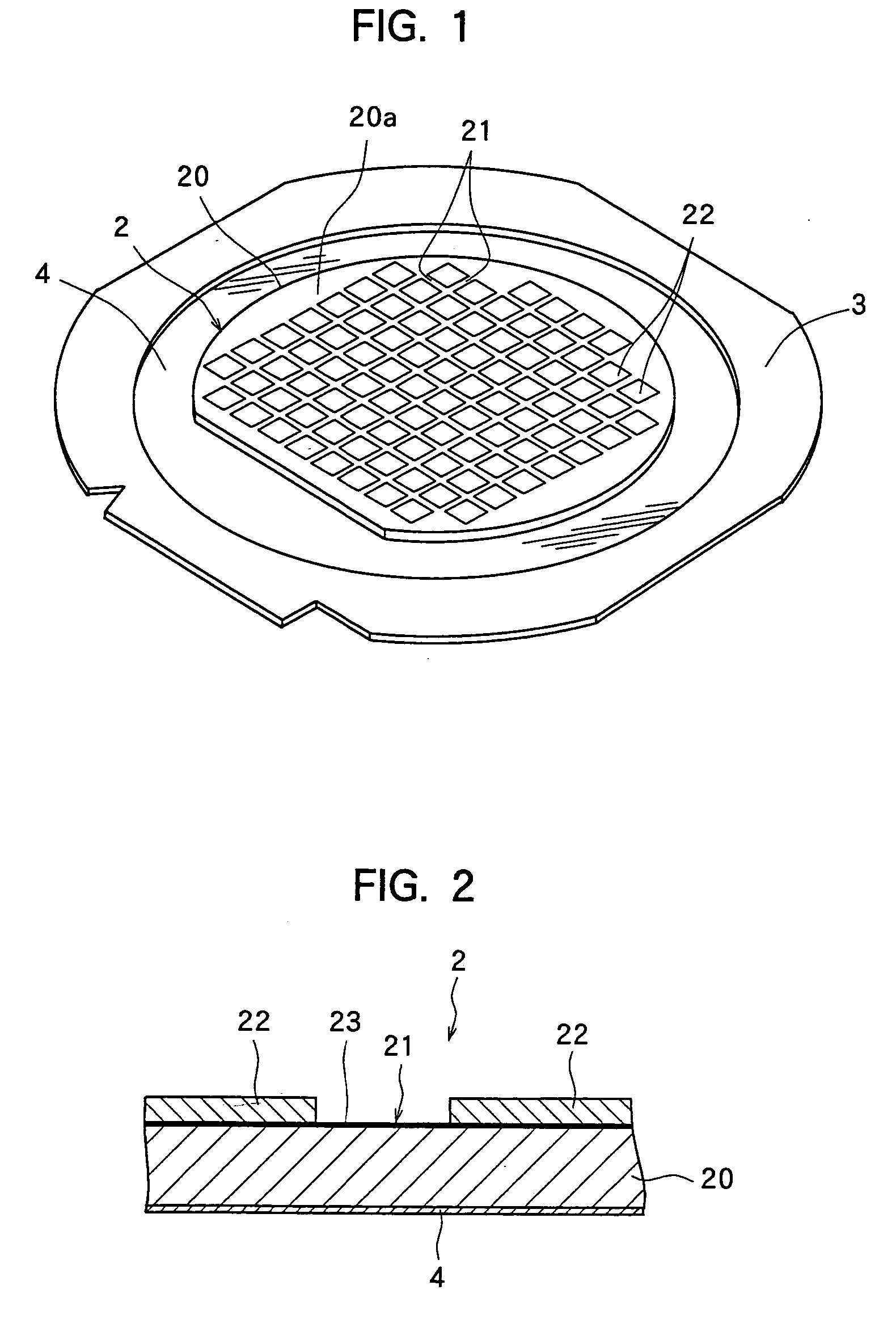
[0024]FIG. 1 is a perspective view of a semiconductor wafer as a plate-like workpiece to be divided according to the present invention. In the semiconductor wafer 2 shown in FIG. 1, a plurality of dividing lines 21 are formed in a lattice pattern on the front surface 20a of a substrate 20 which is a silicon wafer, and a circuit 22 is formed in each of a plurality of areas sectioned by the plurality of dividing lines 21. In the illustrated embodiment, as shown in FIG. 2, a low-dielectric insulating film (Low-k film) 23 composed of a film of an inorganic material such as SiOF or BSG (SiOB) or a film of an organic material such as a polymer exemplified by polyimide or parylene is laminated on the front surface 20a of the substrate 20, and the circuits 22 are formed on the front surface of the Low-k film 23. The...


PUM

PropertyMeasurementUnit
Widthaaaaaaaaaa
Thicknessaaaaaaaaaa

Abstract

A method of dividing a plate-like workpiece having a layer that is made of a different material from that of a substrate and is formed on the front surface of the substrate along predetermined dividing lines, comprising a laser beam application step for applying a laser beam to each dividing line formed on the plate-like workpiece except for a non-processed area in at least one end portion thereof to form grooves deeper than the layer; and a cutting step for cutting the plate-like workpiece along each dividing line by positioning a cutting blade on the side of the non-processed area in the dividing line where the grooves have been formed in the laser beam application step and moving the plate-like workpiece relative to the cutting blade while rotating the cutting blade.

Description

FIELD OF THE INVENTION [0001] The present invention relates to a method of dividing a plate-like workpiece such as a semiconductor wafer or the like. More specifically, it relates to a method of dividing a plate-like workpiece having a layer that is made of a material different from that of a substrate and is formed on the front surface of the substrate, along predetermined dividing lines. DESCRIPTION OF THE PRIOR ART [0002] As is known to people of ordinary skill in the art, in the production process of semiconductor devices, individual semiconductor chips are manufactured by forming a circuit such as IC or LSI in each of a plurality of areas sectioned by dividing lines called “streets” formed in a lattice pattern on the front surface of a substantially disk-like semiconductor wafer and cutting the semiconductor wafer along the dividing lines to divide it into the circuit-formed areas. Cutting along the dividing lines of the semiconductor wafer is generally carried out by a cutting...

Claims


Application Information

Patent Timeline
IPC IPC(8): B23K26/364B28D5/00B23K26/40B23K101/40B28D5/02H01L21/301
CPCB23K26/367B28D5/022B23K2201/40B23K26/4075B23K2101/40B23K2103/50B23K26/364B23K26/40
Inventor NAKAMURA, MASARUYOSHIKAWA, TOSHIYUKIGENDA, SATOSHI
Owner DISCO CORP
Why Eureka
Try Eureka