Stacked chip assembly with stiffening layer

a technology of microelectronic assemblies and stiffening layers, which is applied in the direction of electrical apparatus, semiconductor devices, semiconductor/solid-state device details, etc., can solve the problems of bending, flexing, flopping, etc., and achieves sufficient stiffness and enhance the handling and testability of the sub-assembly

Inactive Publication Date: 2005-02-17
TESSERA INC
View PDF26 Cites 188 Cited by
  • Summary
  • Abstract
  • Description
  • Claims
  • Application Information

AI Technical Summary

Benefits of technology

[0009] The stiffening encapsulant layer is preferably selected from the group consisting of flexibilized epoxies, silicone elastomers, glass sheet, glass-filled epoxies, ceramic materials and plastics. Although the present invention is not limited by any particular theory of operation, it is believed that providing a stiffening layer that surrounds the vertical conductors in the peripheral region of the substrate will enhance handling and testability of the subassembly by providing sufficient stiffness in the peripheral region of the subassembly. Absent the stiffener layer, the peripheral region of the substrate may flex, bend or flop to an undesirable degree during testing and handling.
[0012] In yet further preferred embodiments of the present invention, a microelectronic assembly includes a plurality of microelectronic subassemblies, each subassembly having a substrate with at least one peripheral region, a microelectronic element mounted over the substrate, a plurality of leads electrically connected to the microelectronic element having outer ends overlying the at least one peripheral region of the substrate, vertical conductors electrically connected with the outer ends of the leads, and an encapsulant layer provided over a surface of the substrate and around the vertical conductors for stiffening the substrate at the least one peripheral region of the substrate. The microelectronic subassemblies are stacked one atop another and electrically interconnected through the vertical conductors. The vertical conductors preferably form electrical interconnections between leads of different subassemblies. The vertical conductors preferably include metallic masses, such as solder balls. The microelectronic elements of the assembly may vary in size.

Problems solved by technology

Absent the stiffener layer, the peripheral region of the substrate may flex, bend or flop to an undesirable degree during testing and handling.

Method used


Image

  • Stacked chip assembly with stiffening layer
  • Stacked chip assembly with stiffening layer
  • Stacked chip assembly with stiffening layer

Examples


Embodiment Construction

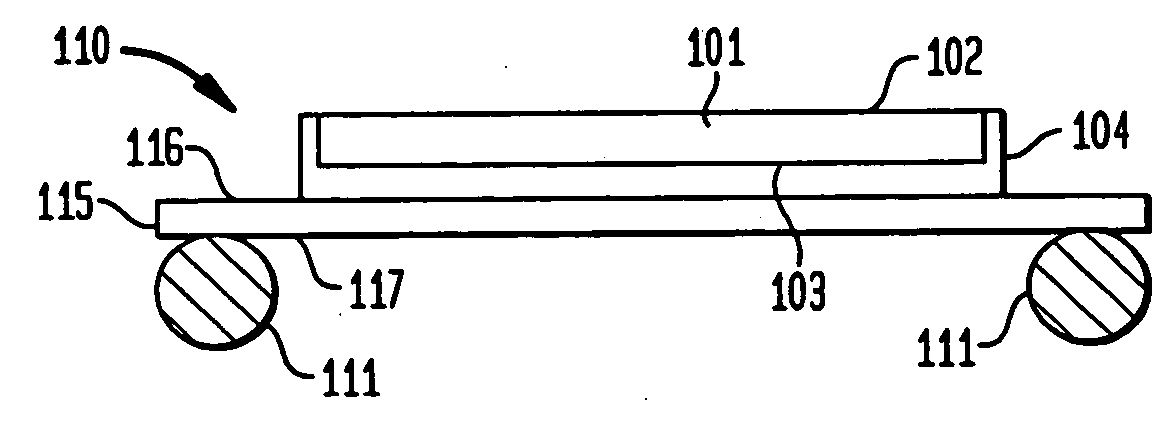
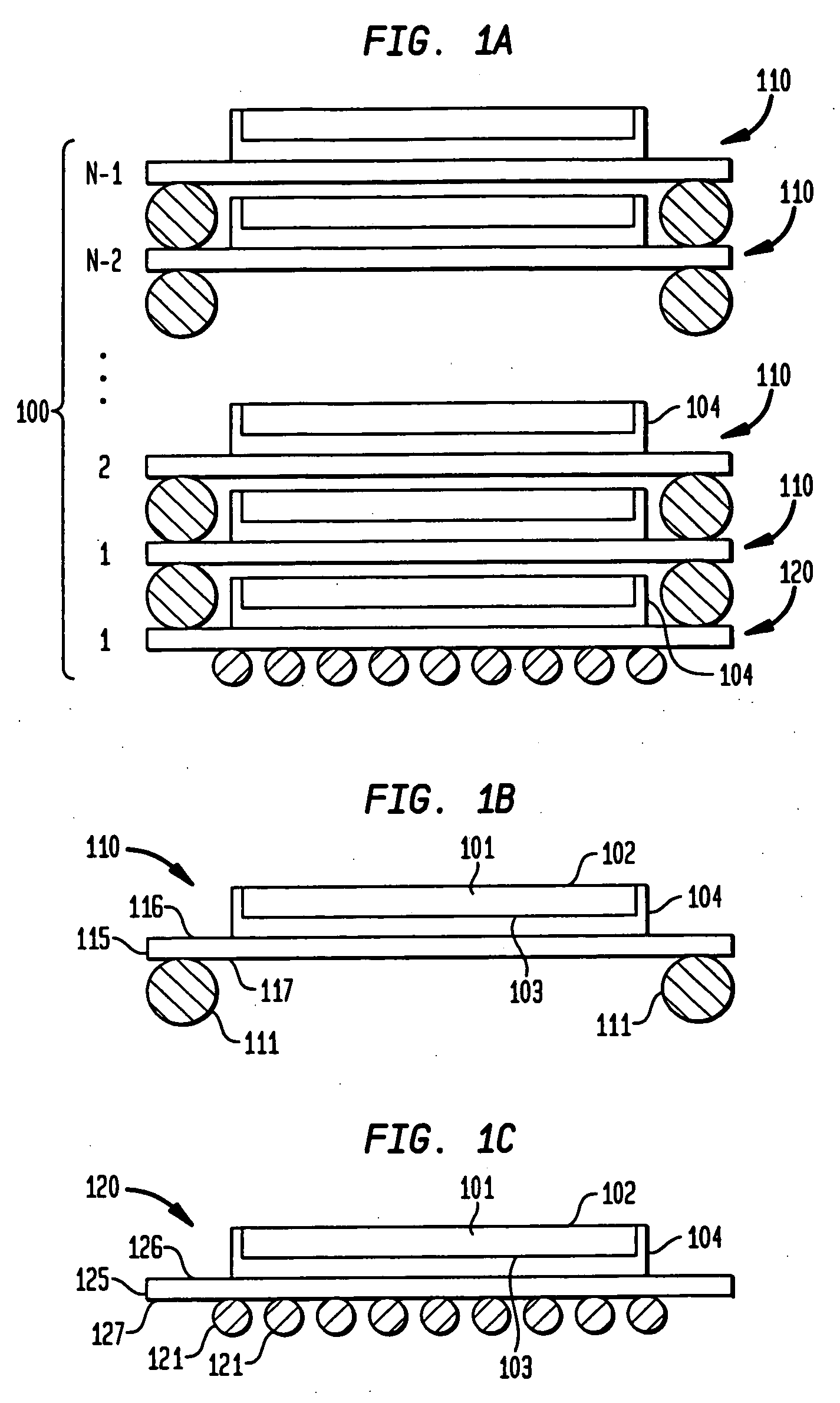
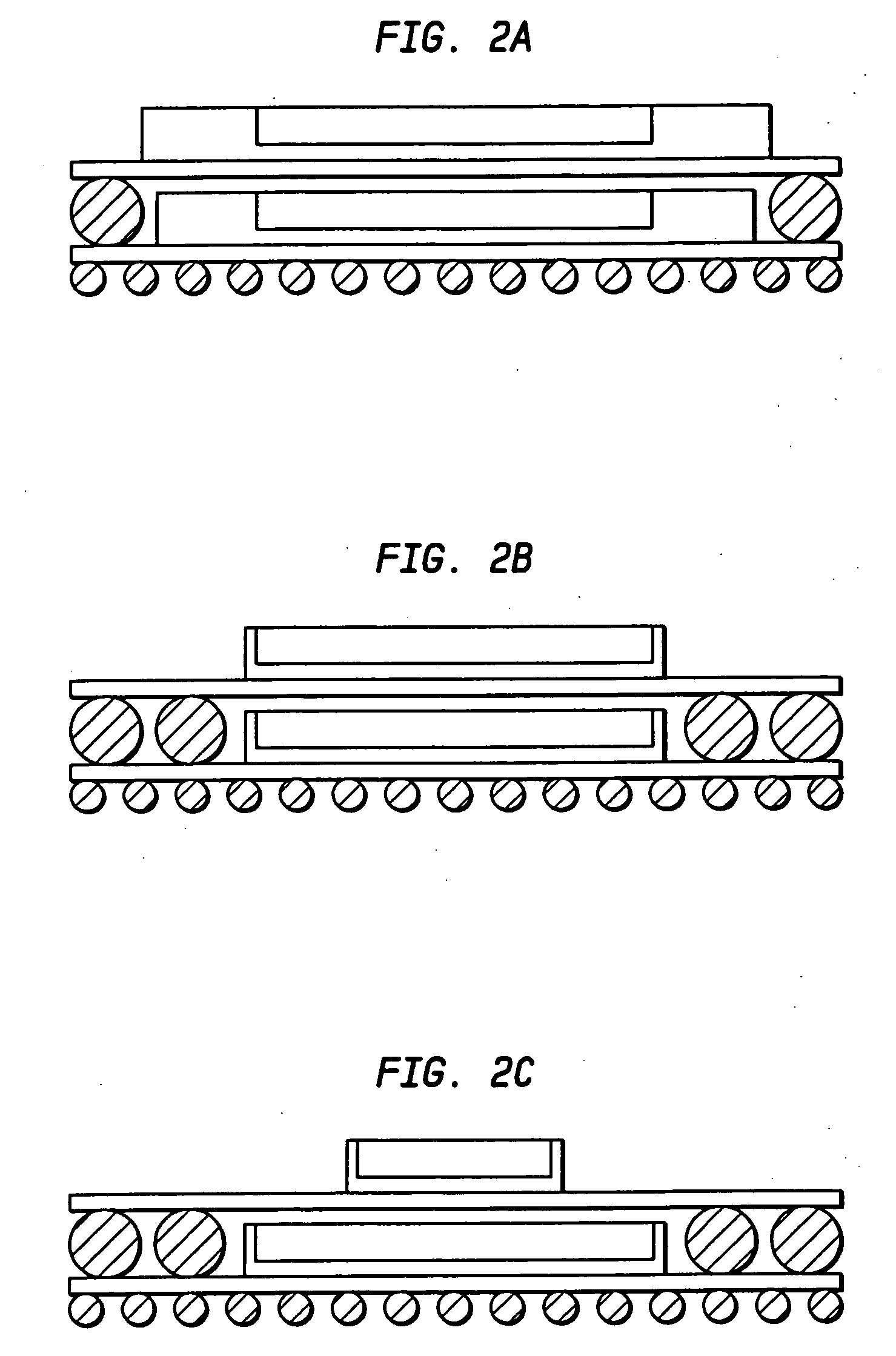
[0036]FIG. 3A illustrates a preferred embodiment of the stacked assembly of the present invention. Stacked assembly 200 includes a plurality of N−1 subassemblies 210 stacked one atop another with a base subassembly 220 occupying the bottom-most position in the stack. Referring to FIGS. 3B and 3C, each subassembly 210, 220 includes a microelectronic element 201, such as a semiconductor chip, having a front face 202, a back face 203 opposite front face 202 and a plurality of contacts 205 exposed at front face 202. Preferably, contacts 205 are exposed in a peripheral region of the chip face. Interposer 215 is desirably a dielectric element having a first surface 216, a second surface 217 opposite first surface 216 and a plurality of conductive pads (not shown) disposed on first surface 216. Interposer 215 also preferably has conductive elements 218 such as metallic traces thereon, with contacts 205 of chip 201 being electrically connected to conductive elements 218. Preferably, interpo...


PUM


Abstract

A microelectronic subassembly 210 includes a substrate 215 having a top surface 216 and at least one peripheral region 219, a microelectronic element 201 mounted over the substrate 215, a plurality of leads 218, 222 electrically connected to the microelectronic element 201 having outer ends overlying the at least one peripheral region 219 of the substrate 215, and vertical conductors 208 electrically connected with the outer ends of the leads. The subassembly includes an encapsulant layer 204 provided over the top surface 216 of the substrate 215 and around the microelectronic element 201 and the vertical conductors 208 for stiffening the substrate 215 at the at least one peripheral region 219 of the substrate for facilitating handling and testing of the subassembly.

Description

TECHNICAL FIELD [0001] The present invention generally relates to stacked microelectronic assemblies, and more particularly relates to stacked microelectronic assemblies having a stiffening layer. BACKGROUND ART [0002] In certain preferred embodiments of commonly assigned U.S. Pat. No. 5,861,666, the disclosure of which is hereby incorporated by reference herein, a stacked microelectronic assembly includes a plurality of chip and interposer subassemblies. Each subassembly has a circuitized interposer and a semiconductor chip, one face of which confronts a surface of the interposer. Each interposer has at least one peripheral region projecting laterally beyond an edge of the chip mounted to the interposer. Each interposer also includes a plurality of leads electrically connected to contacts on the chip face that extend to the peripheral region of the interposer. The subassemblies are stacked one atop another in a generally vertical configuration so that the chips overlie one another ...

Claims


Application Information

Patent Timeline
Patent Type & Authority Applications(United States)
IPC IPC(8): H01L21/56H01L23/16H01L23/31H01L23/498H01L25/10
CPCH01L21/563H01L23/16H01L2224/97H01L2224/48227H01L2225/1058H01L2225/1023H01L2224/73265H01L2224/50H01L2224/32225H01L24/97H01L2924/01322H01L24/48H01L2924/3011H01L2924/15331H01L2924/1532H01L2924/15311H01L2924/09701H01L23/3128H01L23/49816H01L23/4985H01L25/105H01L2224/16H01L2224/48091H01L2224/73203H01L2924/01079H01L2924/00014H01L2924/00012H01L2924/00H01L24/73H01L2924/181H01L2224/05599H01L2224/45099H01L2224/85399H01L2224/45015H01L2924/207
Inventor MOHAMMED, ILYAS
Owner TESSERA INC
Why Eureka
Try Eureka