Semiconductor chip with bumps and method for manufacturing the same

a technology of semiconductors and bumps, applied in the field of semiconductors with bumps, can solve the problems of increasing cost, increasing speed and complexity of ic chips, increasing cost, etc., and achieve the effect of reducing the height of the bumps, without increasing the cost and difficulty of the ball mounting process

Active Publication Date: 2005-02-17
ADVANCED SEMICON ENG INC
View PDF4 Cites 24 Cited by
  • Summary
  • Abstract
  • Description
  • Claims
  • Application Information

AI Technical Summary

Benefits of technology

[0011] In order to achieve the above object, the present invention provides a method for manufacturing a semiconductor chip with bumps. The method comprises providing a semiconductor chip which defines an active surface and a back surface and has a plurality of pads disposed on the active surface, and a plurality of preformed solder balls. A passivation is disposed on the active surface of the semiconductor chip with the pads exposed. A plurality of UBMs (Under Bump Metallurgy) are disposed on the pads and define a plurality of bump pads. The diameter of the bump pads is about 100% to about 130% of the diameter of the preformed solder balls. The preformed solder balls are placed on the bump pads and then reflowed to form a plurality of bumps As described hereinabove, the semiconductor flip chip according to the present invention has a large pad opening to provide a large solder ball wetting area so as to decrease the height of the bumps. The semiconductor flip chip according to the present invention use the comparatively large preformed solder balls in dimensions without increasing the cost and the difficulty of the ball mounting process.

Problems solved by technology

As electronic devices have become smaller and thinner, the speed and the complexity of IC chip become more and more higher.
However, as the size of the solder ball is reduced, the ball mounting process becomes more difficult and the cost also be increased.
In fact, in the prior art, there is no suitable processes for forming the bumps which is 160 μm to 240 μm in height.

Method used


Image

  • Semiconductor chip with bumps and method for manufacturing the same
  • Semiconductor chip with bumps and method for manufacturing the same
  • Semiconductor chip with bumps and method for manufacturing the same

Examples


Embodiment Construction

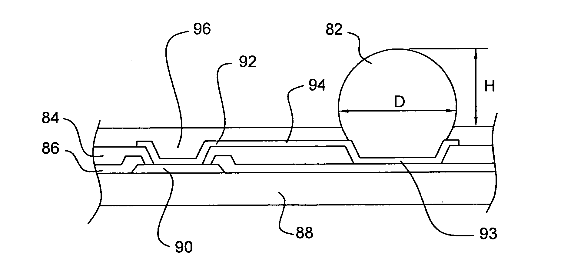
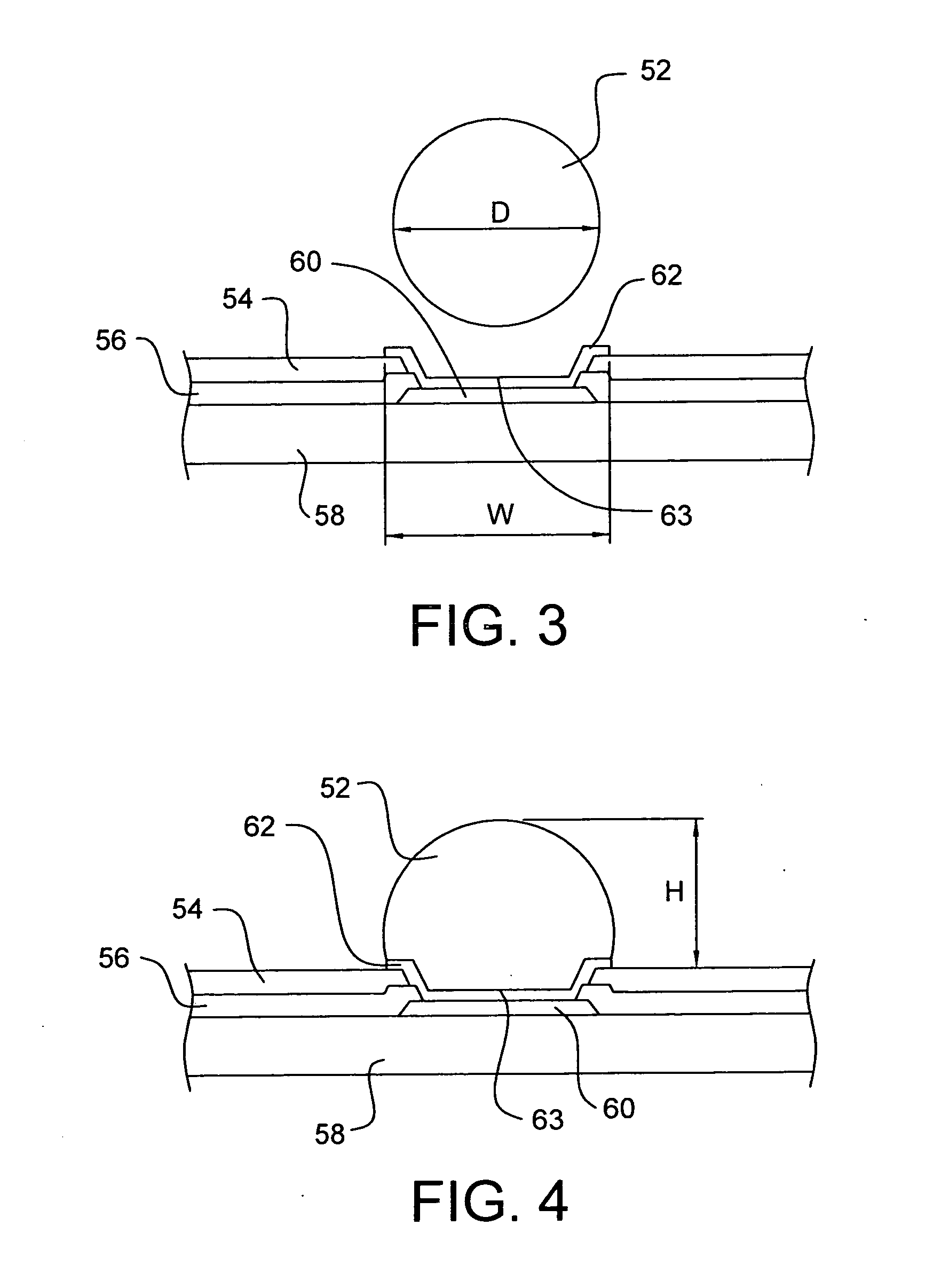
[0019] Referring to FIGS. 3 and 4, they depict a ball mounting process for a semiconductor flip chip 58 according to an embodiment of the present invention. The semiconductor chip 58 has an active surface and a back surface, and is provides with a plurality of pads, such as aluminum pads 60, disposed on the active surface. A passivation layer 56 is disposed on the active surface of the semiconductor chip 58 with the aluminum pads 60 exposed. A repassivation layer 54, for example, such as made of BCB (benzocyclobutene), is disposed on the passivation layer 56 with the aluminum pads 60 exposed. A plurality of UBMs (Under Bump Metallurgy) 62 are disposed on the exposed aluminum pads 60 and define a plurality of bump pads 63.

[0020] A plurality of preformed solder balls 52 are placed on the UBMs 62, i.e. the bump pads 63, and then reflowed to form a plurality of bumps 53. Each of the bump pads 63 defines a pad opening, i.e. the recess area of the UBM 62. Compared with the prior art, the...


PUM

PropertyMeasurementUnit
heightaaaaaaaaaa
diameteraaaaaaaaaa
heightaaaaaaaaaa

Abstract

A method for manufacturing a semiconductor chip with bumps comprises providing a semiconductor chip, which defines an active surface and a back surface and has a plurality of pads disposed on the active surface, and a plurality of preformed solder balls. A passivation is disposed on the active surface of the semiconductor chip with the pads exposed. A plurality of UBMs (Under Bump Metallurgy) are disposed on the pads and define a plurality of bump pads. The diameter of the bump pads is about 100% to about 130% of the diameter of the preformed solder balls. The preformed solder balls are placed on the bump pads and then reflowed to form a plurality of bumps on the semiconductor chip.

Description

BACKGROUND OF THE INVENTION [0001] 1. Field of the Invention [0002] The present invention relates to a semiconductor chip with bumps, and more particularly to a semiconductor chip having a large solder ball wetting area so as to form the bumps of which the height is lower. [0003] 2. Description of the Related Art [0004] As electronic devices have become smaller and thinner, the speed and the complexity of IC chip become more and more higher. Accordingly, a need has arisen for higher packaging efficiency. Demand for miniaturization is the primary catalyst driving the usage of advanced packages such as chip scale packages (CSP) and flip chips. Both of them greatly increase the packaging efficiency and reduce the amount of board real estate required when compared with the alternative ball grid array (BGA) and thin small outline package (TSOP). [0005] The flip chip package itself also has to be miniaturized in dimensions. Specifically, not only the length and the width but also the thic...

Claims


Application Information

Patent Timeline
Patent Type & Authority Applications(United States)
IPC IPC(8): H01L21/60H01L23/498
CPCH01L23/49816H01L2224/05572H01L2924/01013H01L2924/01074H01L2924/01078H01L2924/14H01L2924/01006H01L2924/01033H01L2924/014H01L2924/0002H01L24/13H01L2224/0401H01L2224/11334H01L2224/13007H01L2224/131H01L24/11H01L2224/05552H01L2224/02381H01L2224/05548H01L2224/05124H01L24/05H01L2924/00014
Inventor LIU, CHIH CHIANGPAN, CHI CHENGWANG, KUO LUNGCHEN, CHE HSIUNG
Owner ADVANCED SEMICON ENG INC
Why Eureka
Try Eureka