Immersion fluid for immersion Lithography, and method of performing immersion lithography

a technology of immersion lithography and immersion fluid, which is applied in the field of immersion fluid and a system and method of performing immersion lithography, can solve the problems of hydroxyl ions in photoresists, chemically amplified photoresists, and conventional techniques for improving resolution approaching physical and technical limits

Active Publication Date: 2005-02-17
TAIWAN SEMICON MFG CO LTD
View PDF31 Cites 755 Cited by
  • Summary
  • Abstract
  • Description
  • Claims
  • Application Information

AI Technical Summary

Problems solved by technology

However, these conventional techniques of improving the resolution are approaching physical and technical limits.
Photoresists, particularly chemically amplified photoresists, may be contaminated by hydroxyl ions (OH−) present in the immersion fluid or water.

Method used


Image

  • Immersion fluid for immersion Lithography, and method of performing immersion lithography
  • Immersion fluid for immersion Lithography, and method of performing immersion lithography
  • Immersion fluid for immersion Lithography, and method of performing immersion lithography

Examples


Embodiment Construction

The making and using of the presently preferred embodiments are discussed in detail below. It should be appreciated, however, that the present invention provides many applicable inventive concepts that can be embodied in a wide variety of specific contexts. The specific embodiments discussed are merely illustrative of specific ways to make and use the invention, and do not limit the scope of the invention.

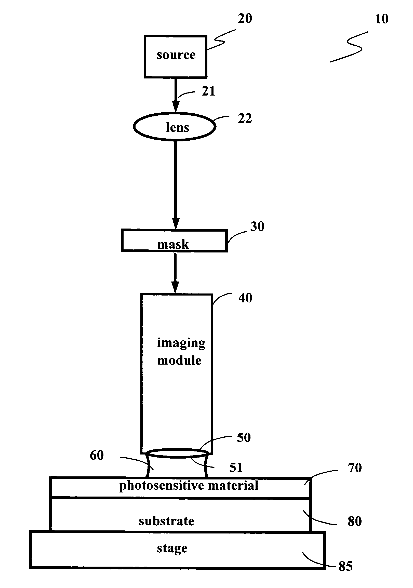
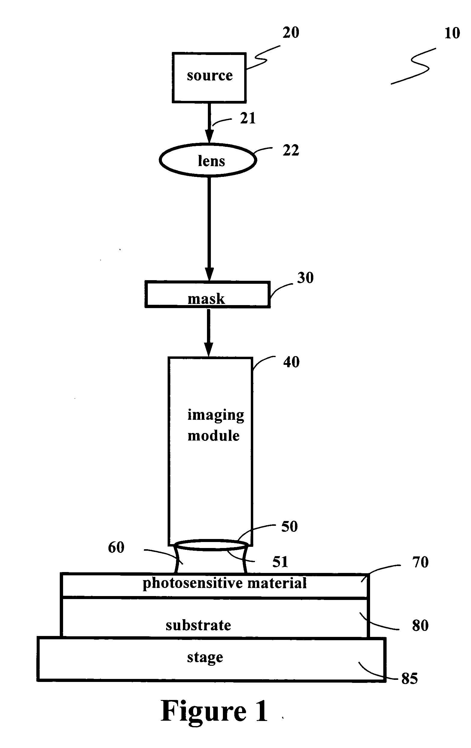
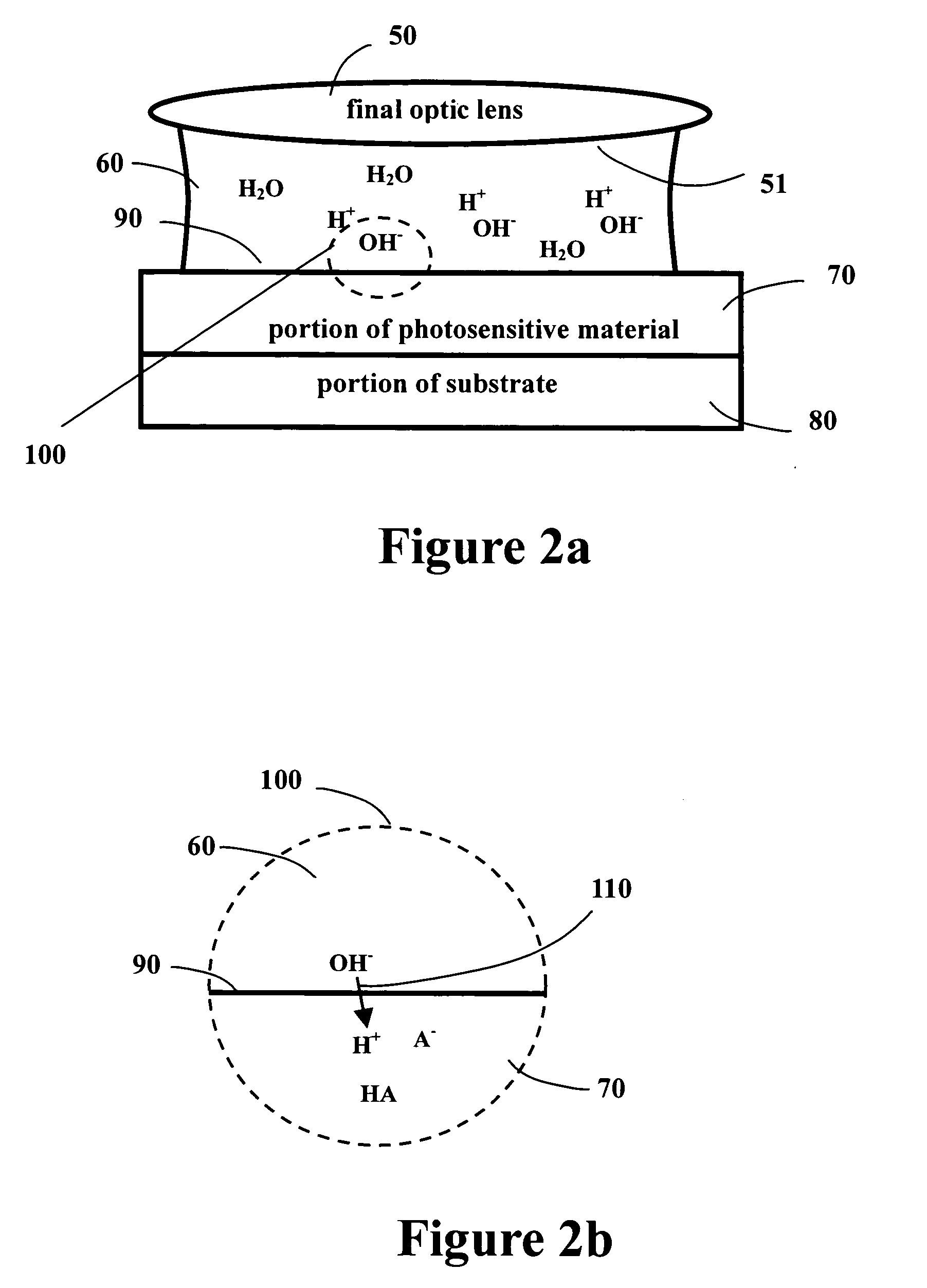
A simplified example of an immersion lithography system 10 is illustrated in FIG. 1. System 10 contains a source 20 emitting a beam of optical energy 21 through a lens 22. The energy is then passed through a mask 30 and an imaging module 40, and a final lens 50 having an optical surface 51. A fluid 60 fills at least the space between lens 50 and a photosensitive material 70. Photosensitive material 70 is in contact with a substrate 80 of a semiconductor device.

In the preferred embodiment, the substrate 80 is a semiconductor substrate that is being fabricated as an integrated c...


PUM

PropertyMeasurementUnit
gate lengthaaaaaaaaaa
wavelengthaaaaaaaaaa

Abstract

An immersion lithographic system 10 comprises an optical surface 51, an immersion fluid 60 with a pH less than 7 contacting at least a portion of the optical surface, and a semiconductor structure 80 having a topmost photoresist layer 70 wherein a portion of the photoresist is in contact with the immersion fluid. Further, a method for illuminating a semiconductor structure 80 having a topmost photoresist layer 70 comprising the steps of: introducing an immersion fluid 60 into a space between an optical surface 51 and the photoresist layer wherein the immersion fluid has a pH of less than 7, and directing light preferably with a wavelength of less than 450 nm through the immersion fluid and onto the photoresist.

Description

TECHNICAL FIELD The present invention relates generally to the fabrication of semiconductor devices, and more particularly to an immersion fluid and a system and method for performing immersion lithography. BACKGROUND In photolithographic systems, there is a need to achieve a high resolution in order to resolve high-resolution patterns, such as images, lines, or spots. In a photolithographic system employed in the integrated circuit (IC) industry, light is projected onto a resist for the purpose of patterning an electronic device. Photolithographic systems have been used in the IC industry for many decades and are expected to resolve line widths of 50 nm and below in the future. Significant improvement in the resolution of photolithographic systems has been one of the most important enablers for the manufacture of high density and high-speed semiconductor IC chips. The resolution R of a photolithographic system for a given lithographic constant k1, is given by R=k1λ / NA, where λ i...

Claims


Application Information

Patent Timeline
Patent Type & Authority Applications(United States)
IPC IPC(8): G03F7/20
CPCG03F7/70341
Inventor YEO, YEE-CHIALIN, BURN-JENGHU, CHENMING
Owner TAIWAN SEMICON MFG CO LTD
Why Eureka
Try Eureka