Semiconductor device, and a method for manufacturing the same

a technology of semiconductor devices and semiconductors, applied in the direction of semiconductor devices, electrical equipment, transistors, etc., can solve the problems of affecting the production yield and uniformity of characteristics of the obtained tfts, affecting the production efficiency of tfts, etc., to achieve high resistivity and high resistivity. region

Inactive Publication Date: 2005-02-24
SEMICON ENERGY LAB CO LTD
View PDF49 Cites 9 Cited by
  • Summary
  • Abstract
  • Description
  • Claims
  • Application Information

AI Technical Summary

Benefits of technology

[0006] It is an object of the present invention to improve the quality of TFTs and the manufacturing yield by solving the foregoing problems. Specifically, it is an object of the present invention to prevent degradation caused by hot carriers, and to produce a high resistivity region in a self-aligning manner without using a photolithography process.
[0011] In FIG. 1, an N- region 111 is interposed between a source region 110 having an N-type and a channel region 3. A gate insulating film 104 exists on the N- region 111. Further, a silicon nitride film 114 which is capable of trapping positive ions therein is formed on the source region and the gate insulating film 104. It is to be understood that even if hot electrons are injected into the gate insulating film from the active layer close to the source region, these can be neutralized by the positive charges existing in the silicon nitride film 114. Accordingly, the high resistivity region can function correctly. Also, the TFT shown in FIG. 1 includes an offset region between the channel region 3 and the high resistivity region 111. The offset region is an extension of the channel region and has a same conductivity type as the channel region (intrinsic).

Problems solved by technology

However, negative charges caused by hot carriers in an N-channel type TFT tend to be trapped in a portion of a gate insulating film close to a drain region so that the conductivity type of the high resistivity region shifts to p-type.
As a result, the source / drain current is obstructed.
This means that production yield and a uniformity of characteristics in the obtained TFTs can not be improved.

Method used


Image

  • Semiconductor device, and a method for manufacturing the same
  • Semiconductor device, and a method for manufacturing the same
  • Semiconductor device, and a method for manufacturing the same

Examples


example 1

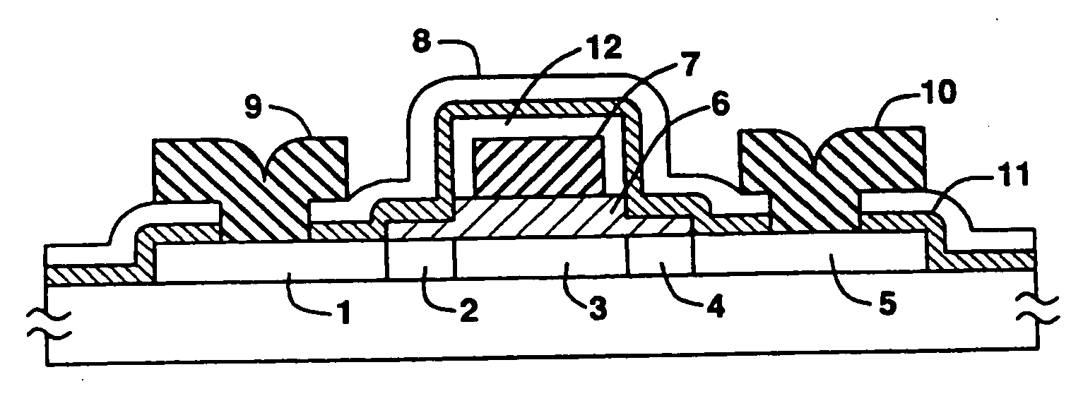
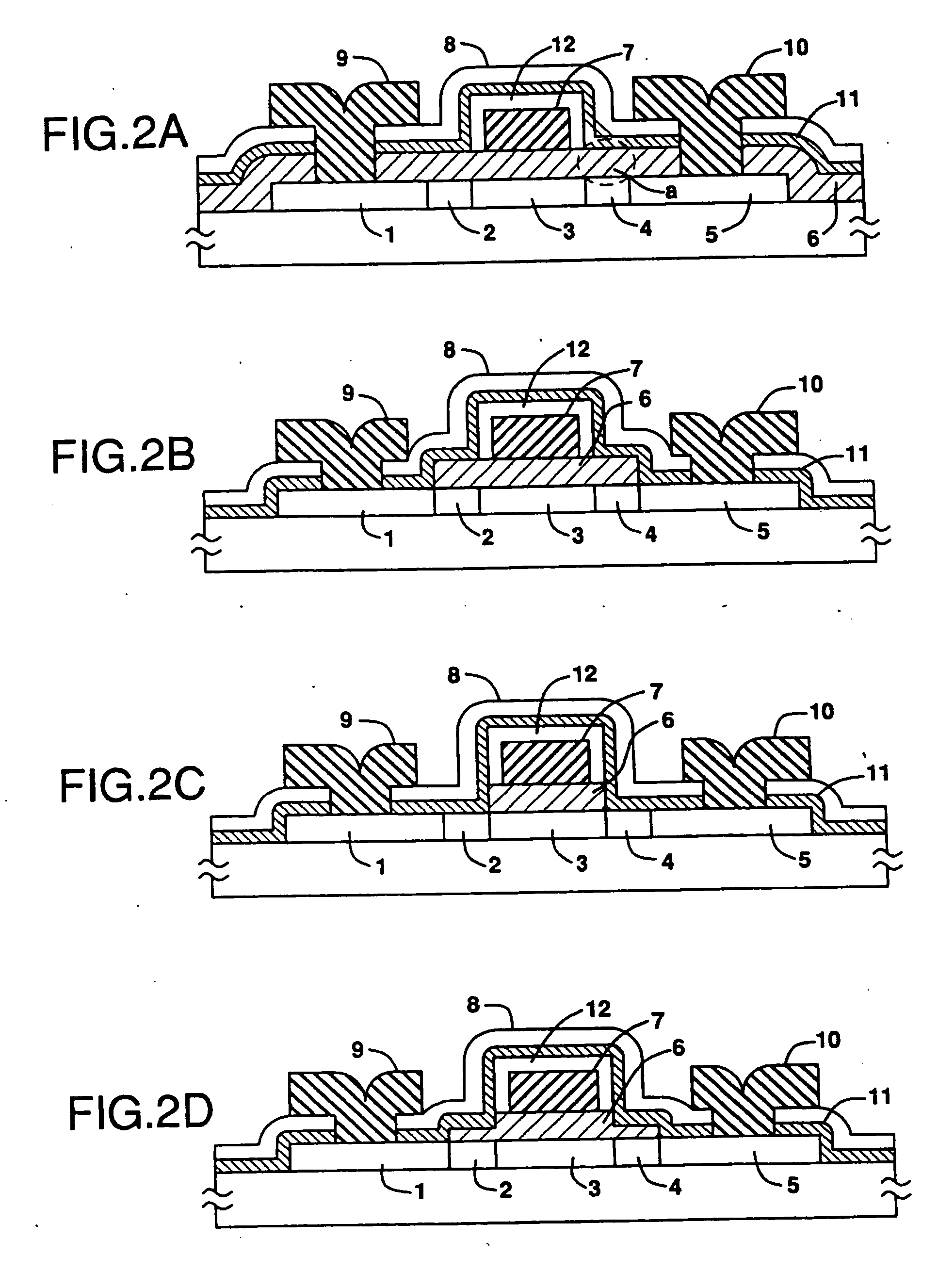
[0036] A manufacturing process of a TFT in accordance with the present invention will be explained with reference to FIGS. 3A to 3H.

[0037] Initially, a non-alkaline glass substrate 101, for example, Corning 7059 (300 mm×400 mm or 100 mm×100 mm) is coated with a silicon oxide film 102 of 1000-3000 Å thick. The Silicon oxide film may be formed by sputtering in an oxygen atmosphere. However, it is preferable to use a plasma CVD with a TEOS (tetra ethoxy silane) gas used as a starting material to improve the productivity. In place of silicon oxide, other materials may be used. For example, a single layer of aluminum nitride, a double layer of silicon nitride and aluminum nitride. Aluminum nitride may be formed by a reactive sputtering in a nitrogen atmosphere.

[0038] Then, an active layer 103, for example, crystalline silicon is formed on the silicon oxide film 102. The “crystalline silicon” in this invention may be any form of silicon if it includes crystals at least partly, for examp...

example 2

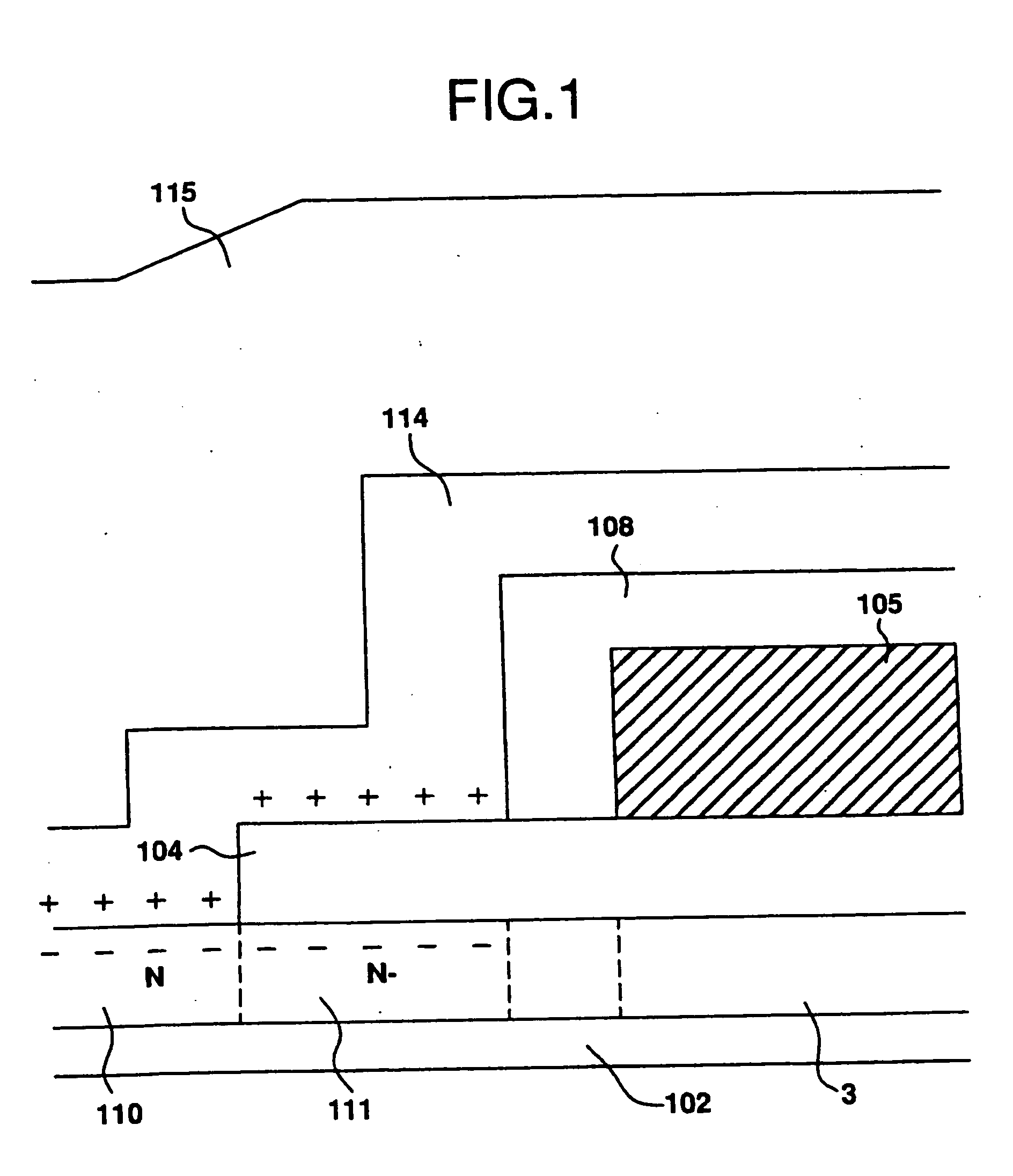
[0063] This example employs the same process as described in the first example until the structure shown in FIG. 3E is obtained. Thus, redundant explanations will be omitted. However, the thickness of the insulating film 104 in this example is thicker than that in the first example. For example, the insulating film is 1000-1500 Å thick, for example, 1200 Å, so that a gate leak current can be minimized and it can be endure a high voltage during the anodic oxidation.

[0064] Referring to FIG. 4A which corresponds to FIG. 3E, ion doping of nitrogen ions is carried out using the gate electrode and the insulating film 104′ as a mask at a dose of 1×10¹⁴-3×10¹⁶ atoms / cm2, for example, 2×10¹⁵ and with an acceleration voltage of 50-100 kV, for example, 80 kV. The acceleration voltage is made so high that the nitrogen ions almost pass through the regions 110 and 113 of the active layer on which the insulating film 104′ does not exist. Accordingly, the regions 110 and 113 are not effectively do...

example 3

[0071] Referring to FIG. 6A, in the same manner as in the first example, an underlying film comprising silicon oxide 102, an island form silicon film 103 of 800 Å having a crystallinity, a silicon oxide film 104 of 1200 Å, a gate electrode 105 made of aluminum of 200 nm—1 μm thick, and a porous anodic oxide film 107 (3000 Å—1 μm , e.g. 5000 Å thick) on the side surface of the gate electrode are formed on a Corning 7059 glass substrate 101.

[0072] Further, a barrier type anodic oxide film 108 is formed to a thickness of 1000-2500 Å in the manner as in the first example. (FIG. 6B).

[0073] Using the porous anodic oxide 107 as a mask, the silicon oxide film 104 is etched into a gate insulating film 104′. Then, using the barrier type anodic oxide 108 as a mask, the porous anodic oxide 107 is etched off. Subsequently, an impurity element is introduced by ion doping using the gate electrode with the barrier type anodic oxide formed thereon and the gate insulating film used as a mask, there...


PUM


Abstract

A thin film transistor of the present invention has an active layer including at least source, drain and channel regions formed on an insulating surface. A high resistivity region is formed between the channel region and each of the source and drain regions. A film capable of trapping positive charges therein is provided on at least the high resistivity region so that N-type conductivity is induced in the high resistivity region. Accordingly, the reliability of N-channel type TFT against hot electrons can be improved.

Description

BACKGROUND OF THE INVENTION [0001] The preset invention relates to a semiconductor device and a manufacturing method for the same. In particular, the present invention is directed to an insulated gate field effect transistor (TFT) formed on an insulating surface, for example, a surface of an insulating substrate such as glass, or an insulating film such as silicon oxide formed on a silicon wafer. Also, the present invention is advantageous for the formation of an insulated gate field effect transistor, especially of an N-channel type, which is driven at a relatively high voltage. It is also to be understood that the present invention is further advantageous for the formation of a TFT on a glass substrate of which glass transition temperature (i.e. distortion point) is 750° C. or lower. [0002] Moreover, the present invention is related to an active matrix of a liquid crystal device, a driving circuit of an image sensor or a three dimensional integrated circuit (hybrid IC) using the f...

Claims


Application Information

Patent Timeline
Patent Type & Authority Applications(United States)
IPC IPC(8): H01L21/336H01L21/77H01L21/84H01L27/13H01L29/786
CPCH01L29/66757H01L29/78621H01L27/1248H01L2029/7863H01L27/1255H01L29/772
Inventor TAKEMURA, YASUHIKOTERAMOTO, SATOSHI
Owner SEMICON ENERGY LAB CO LTD
Why Eureka
Try Eureka