Eureka AIR delivers breakthrough ideas for toughest innovation challenges, trusted by R&D personnel around the world.

Contact pin and socket for electrical parts

Inactive Publication Date: 2005-02-24
ENPLAS CORP
View PDF9 Cites 4 Cited by
  • Summary
  • Abstract
  • Description
  • Claims
  • Application Information

AI Technical Summary

Benefits of technology

[0012] An object of the present invention is to substantially eliminate defects or drawbacks encountered in the prior art mentioned above and to provide a contact pin used for a socket for electrical parts having an improved structure of an elastic portion of the contact pin and also provide a socket for electrical parts having such improved contact pin.
[0017] According to this aspect, the elastic portion of the contact pin is formed to have a smooth surface by the polishing means, so that a load is not concentrated at a specific portion even if the load is repeatedly applied, and hence, the durability of the contact pin can be improved.
[0020] According to the preferred embodiment mentioned above, the contact pin even being small in size and weak in strength can be polished, by such as chemical polishing, by applying no external mechanical force. According to the chemical polishing treatment, a number of contact pins can be polished at the same time by, for example, dipping them in a polishing solution, thus improving the workability for manufacturing the contact pins. The nickel plating will compensate the reduction in thickness of the contact pin including the elastic portion through the polishing treatment and, hence, the elastic strength of the elastic portion will be maintained.

Problems solved by technology

However, in the known structure mentioned above, there may cause a case that a rough or course cut surface may be provided at the time of punching out the contact pin from the metal thin plate, and, in such case, according to the repeated operation of accommodation or removal of the IC package, the elastic portion of the contact pin may be loaded repeatedly and a stress is concentrated on a corner portion thereof by the coarse surface of the elastic portion, thus facilitating fatigue and making worse its durability.

Method used


Image

  • Contact pin and socket for electrical parts
  • Contact pin and socket for electrical parts
  • Contact pin and socket for electrical parts

Examples


Embodiment Construction

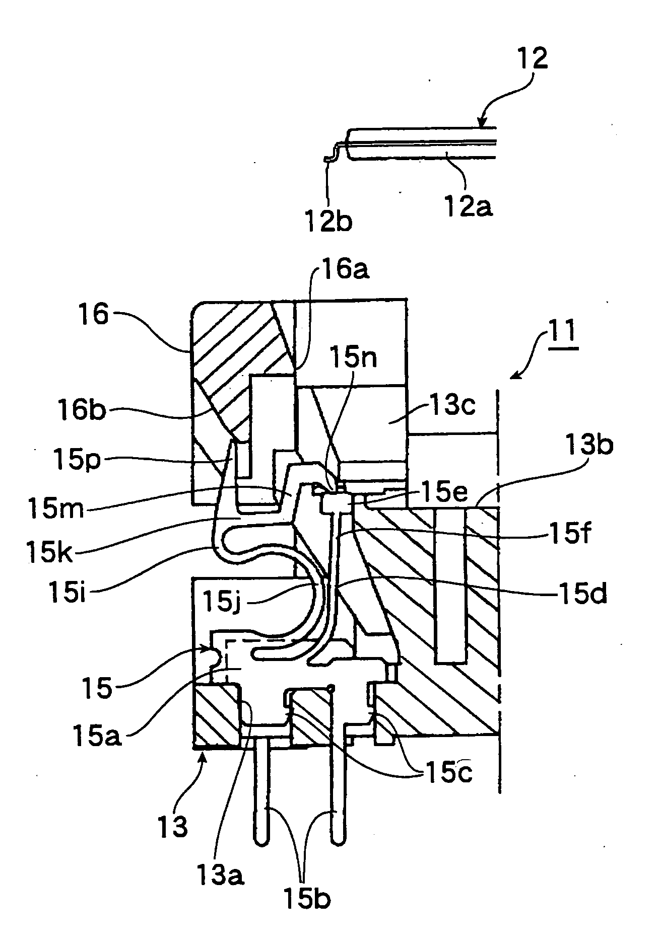
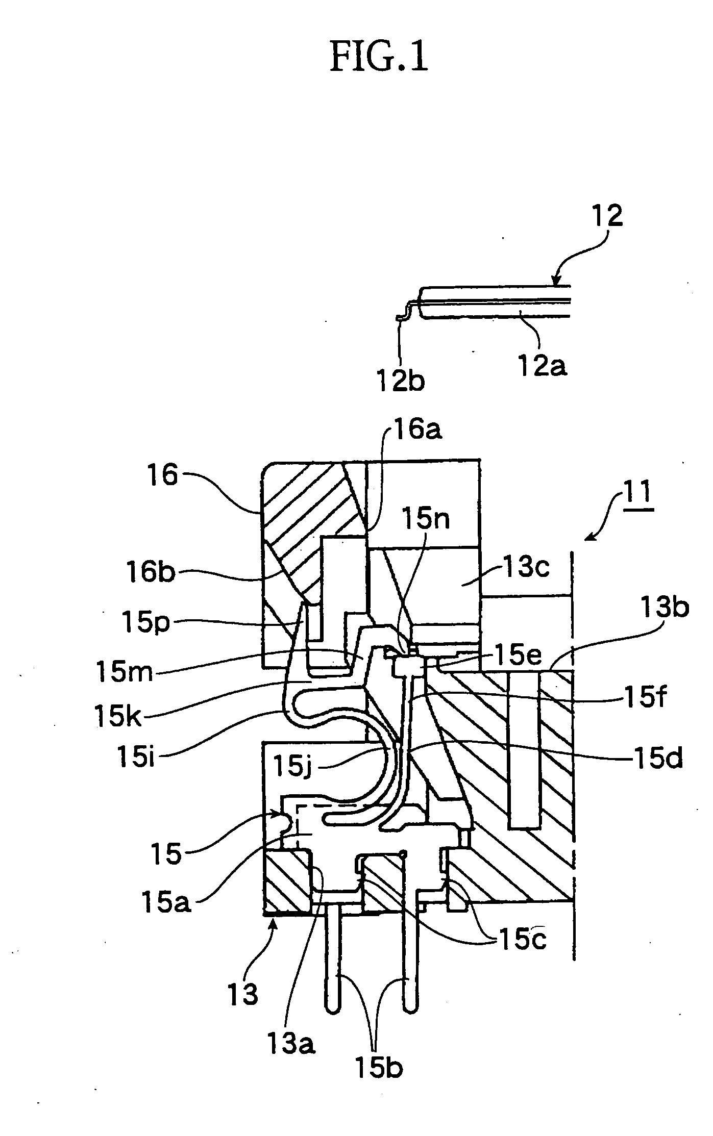
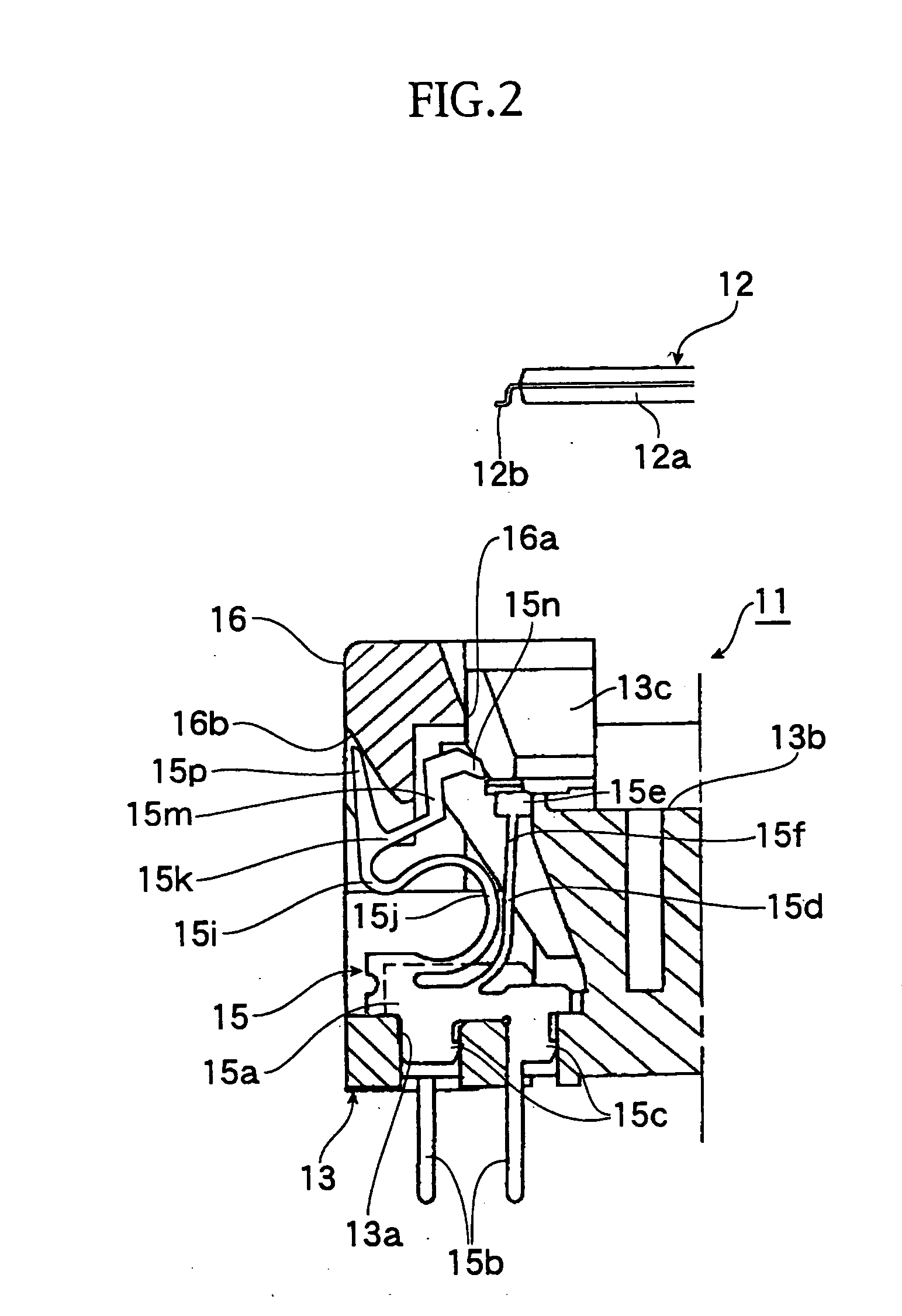
[0040] A preferred embodiment of the present invention will be described hereunder with reference to the accompanying drawings of FIGS. 1 to 5.

[0041] With reference to FIG. 1, an IC socket as “a socket for electrical parts” is totally designated by reference numeral 11, and the IC socket 11 is utilized for electrical connection between an IC lead 12b as “a terminal” for an IC package 12 as “an electrical part” and a printed circuit board (not shown) of a tester, in order to carry out a performance test of the IC package 12.

[0042] The IC package 12 is, as shown in FIG. 1, so-called a gull-wing-type, having a structure in which a number of IC leads 12b project sideways from a rectangular package body 12a of the IC package 12.

[0043] On the other hand, the IC socket 11 generally has a socket body 13 to be mounted on a printed circuit board, not shown, and the socket body 13 is formed with a number of contact pins 15 which are elastically deformable and connected to be electrically co...


PUM


Abstract

A contact pin for an IC socket. The contact pin is formed from a metal material having conductivity and includes an elastic portion that is elastically deformable by a force applied thereto. A contact portion is formed at an end portion of the elastic portion and contacts an IC lead of an IC package. The elastic portion is polished to improve durability.

Description

CROSS REFERENCE TO RELATED APPLICATIONS [0001] This application is a divisional of U.S. application Ser. No. 10 / 151,000, now allowed. This application also claims the benefit of Japanese Application No. 2001-152926, filed May 22, 2001 and Application No. 2001-158525, filed May 28, 2001, in the Japanese Patent Office, the disclosures of which are incorporated herein by reference.BACKGROUND OF THE INVENTION [0002] 1. Field of the Invention [0003] The present invention relates to a contact pin utilized for a socket for electrical parts for detachably accommodating and holding an electrical part such as a semiconductor device (called as “IC package” hereinlater), and also related to a socket for electrical parts provided with such contact pin. [0004] 2. Related Art of the Invention [0005] In a known art, there has been provided an IC socket, as “socket for electrical parts” mentioned above, for carrying out performance test of an IC package as “electrical part”, which is preliminarily d...

Claims


Application Information

Patent Timeline
IPC IPC(8): G01R31/26G01R1/073H01R4/26H01R12/89H01R13/11H01R13/631H01R33/76H05K7/10
CPCH01R4/26H01R12/89H05K7/1023H01R33/76
Inventor MIURA, AKIRA
Owner ENPLAS CORP
Why Eureka
Eureka Blog
Learn More