Semiconductor device with pipe for passing refrigerant liquid

a technology of semiconductor devices and liquid refrigerant, which is applied in the direction of semiconductor devices, semiconductor/solid-state device details, electrical equipment, etc., to achieve the effects of reducing size and cost, improving performance, and increasing the amount of conducting curren

Active Publication Date: 2005-03-03
MITSUBISHI ELECTRIC CORP
View PDF10 Cites 20 Cited by
  • Summary
  • Abstract
  • Description
  • Claims
  • Application Information

AI Technical Summary

Benefits of technology

[0009] According to the semiconductor device of the present invention, 1) performance improvement (an increase in the amount of a conducting current) of the device may be realized because the power semiconductor element which

Problems solved by technology

This sort of structure has been an obstacle in seeking size reduction of the device while fur

Method used


Image

  • Semiconductor device with pipe for passing refrigerant liquid
  • Semiconductor device with pipe for passing refrigerant liquid
  • Semiconductor device with pipe for passing refrigerant liquid

Examples


first preferred embodiment

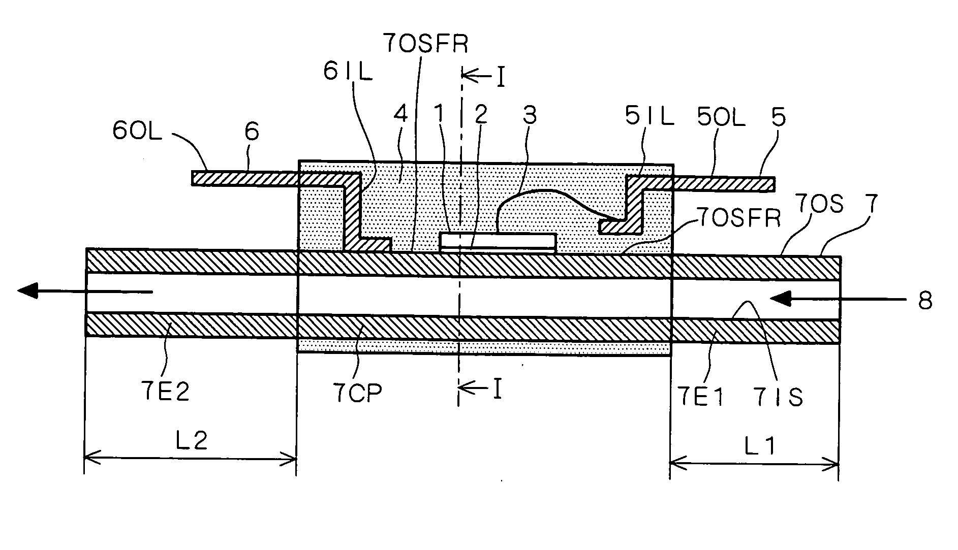
[0017]FIG. 1 is a vertical sectional view of a structure of a power semiconductor device according to the present preferred embodiment. FIG. 2 is a view showing a part in an enlarged manner of a vertical sectional structure taken along the line I-I of FIG. 1.

[0018] In FIGS. 1 and 2, a conductive pipe 7 is made of a conductive material (a metal body, an alloy and the like), which is a thin conductive tubular body (a metallic pipe and the like) including 1) an inner surface 7IS forming an inner space shaping a path of an insulative cooling refrigerant liquid 8, and 2) an outer surface 7OS having a plane (also referred to as a plane portion or a plane region) 7OSFR partially formed thereof. A vertical section of the conductive pipe 7 can take an arbitrary shape, and the plane portion 7OSFR may be formed by, for example, pressing a portion of an outer surface having a vertical section of a round shape of a conductive pipe with a press.

[0019] A power semiconductor element or power semi...

first modification

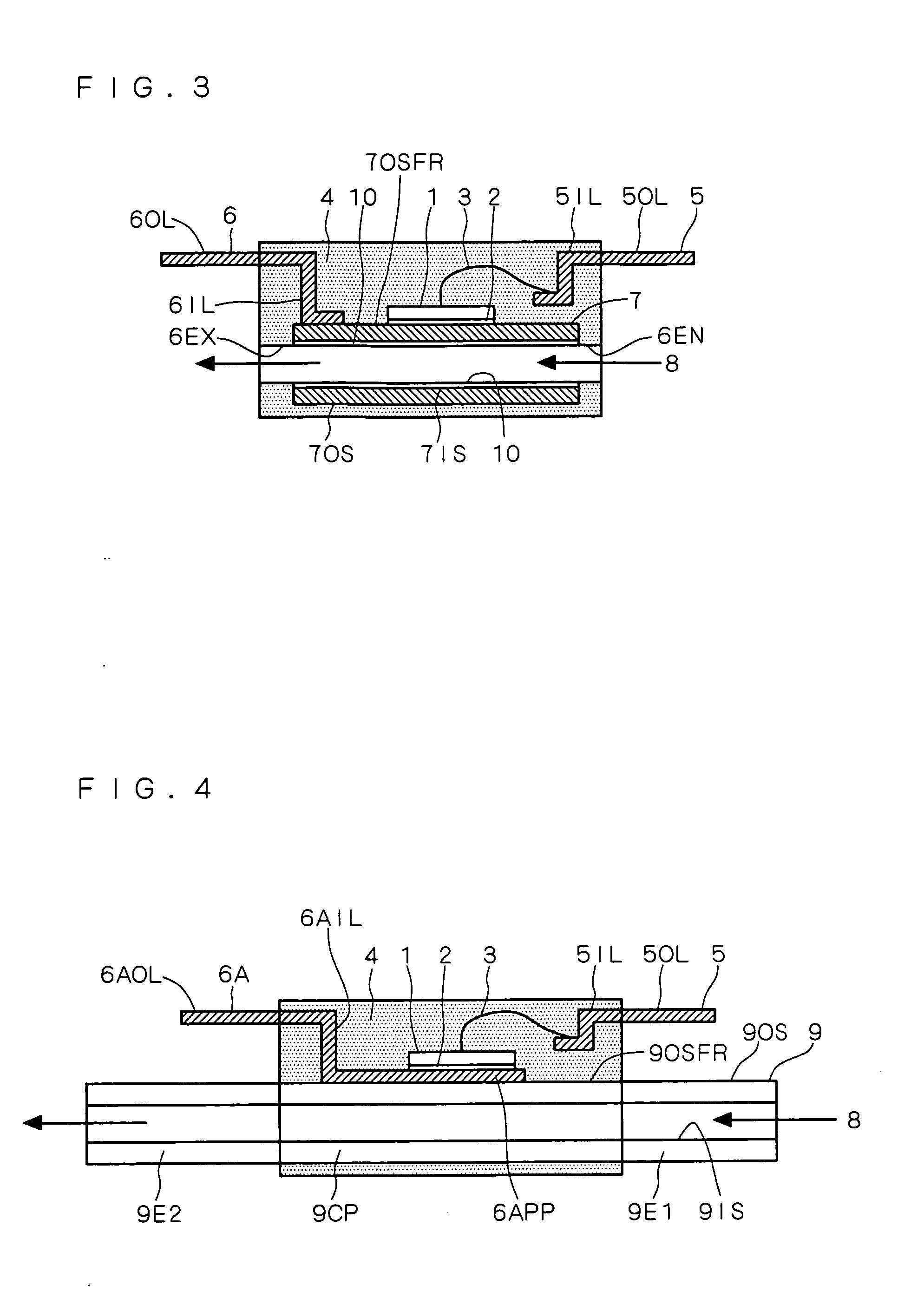
[0026] The present modification is an improvement of the semiconductor device according to the first preferred embodiment. The features of this device are that 1) the conductive pipe 7 further includes an insulating film 10 formed on the whole of the inner surface 7IS, 2) the mold resin 4 covers the whole of the conductive pipe 7, and 3) the mold resin 4 includes a refrigerant liquid inlet 6EN continuous with one end portion of the conductive pipe 7 and a refrigerant liquid outlet 6EX continuous with the other end portion of the conductive pipe 7. Those features will now be described in detail with reference to the drawing.

[0027]FIG. 3 is a vertical sectional view of a structure of a semiconductor device according to the present modification. The structure shown in FIG. 3 differs from that shown in FIG. 1 in the following respects. Namely, the whole of the conductive pipe 7 is buried in the mold resin 4 by the transfer mold process. Additionally, two holes are formed in side surfac...

second preferred embodiment

[0028]FIG. 4 is a vertical sectional view of a structure of a power semiconductor device according to the present preferred embodiment. One of the features which structurally distinguishes the present device from the device shown in FIG. 1 according to the first preferred embodiment is that A) an insulative pipe 9 is used instead of the conductive pipe 7, which includes an inner surface 9IS forming an inner space shaping a path of the cooling refrigerant liquid 8 (which may be an insulative substance, or alternatively, a conductive substance such as inexpensive water) and an outer surface 9OS having a plane region 9OSFR partially formed thereof. The plane portion 9OSFR may be formed on a central portion 9CP as well as either or both of end portions 9E1 and 9E2. Thanks to this structure, B) a first external connecting terminal 6A includes an inner lead part 6AIL including a pad part 6APP bonded onto the plane 9OSFR of the insulative pipe 9 and an outer lead part 6AOL continuous with ...


PUM


Abstract

A semiconductor device includes 1) a conductive pipe including an inner surface forming an inner space shaping a path of an insulative cooling refrigerant liquid and an outer surface including a plane potion partially formed thereof, 2) a power semiconductor element fixed onto the plane portion of the conductive pipe through a bonding layer such as solder, 3) a first external connecting terminal including an inner lead part including a tip portion bonded onto the plane portion of the conductive pipe and an outer lead part continuous with the inner lead part, 4) a second external connecting terminal which is in the state of floating above the outer surface, and 5) a mold resin covering the whole surface of the power semiconductor element, the whole of the inner lead parts of the external connecting terminals, and the whole of the outer surface covering a central portion of the conductive pipe.

Description

BACKGROUND OF THE INVENTION [0001] 1. Field of the Invention [0002] The present invention relates to a cooling technique of a power semiconductor device. [0003] 2. Description of the Background Art [0004] In order to dissipate heat generated from a power semiconductor element to the exterior, a conventional power semiconductor device has a copper plate bonded to a back surface of the power semiconductor element with a brazing material and a ceramic plate bonded to the copper plate with a brazing material provided therein, a back surface of the ceramic plate being in contact with an external cooling system (a cooling plate having a path for passing a refrigerant liquid formed therein) through adhesion grease. The conventional power semiconductor device is disclosed in Japanese Patent Application Laid-Open Nos. 2002-270748, 2002-093974 and 2001-332679. [0005] In the conventional semiconductor device, members for the copper plate and the ceramic plate need to be used to attach the cool...

Claims


Application Information

Patent Timeline
IPC IPC(8): H01L23/433H01L23/473
CPCH01L23/4334H01L23/473H01L2224/48247H01L24/48H01L2924/13055H01L2224/48091H01L2924/1305H01L2224/32245H01L2224/73265H01L2924/13091H01L2924/00H01L2924/00014H01L2924/181H01L2924/00012H01L2224/45099H01L2224/45015H01L2924/207
Inventor ANDOU, KATSUJI
Owner MITSUBISHI ELECTRIC CORP
Why Eureka
Try Eureka