Semiconductor integrated circuit

a technology of integrated circuits and semiconductors, applied in the direction of instruments, digital transmission, generating/distributing signals, etc., can solve problems such as malfunctions, and achieve the effects of high accuracy, stable operation and high accuracy

Active Publication Date: 2005-03-03
RENESAS ELECTRONICS CORP
View PDF4 Cites 144 Cited by
  • Summary
  • Abstract
  • Description
  • Claims
  • Application Information

AI Technical Summary

Benefits of technology

The technology described in this patent allows for accurate and stable synchronization between different components in a computer system without interference caused by electrical reflections. This results in more reliable performance even at varying temperatures. Additionally, the technology includes mechanisms that allow for easy re-calibration of timings during normal operations, reducing the likelihood of failures in the final product.

Problems solved by technology

The technical problem addressed by this patent is how to synchronize the timing between a memory interface controller that controls aDDR-SDRAM and its own internal clock.

Method used


Image

  • Semiconductor integrated circuit
  • Semiconductor integrated circuit
  • Semiconductor integrated circuit

Examples


Embodiment Construction

[0051]>

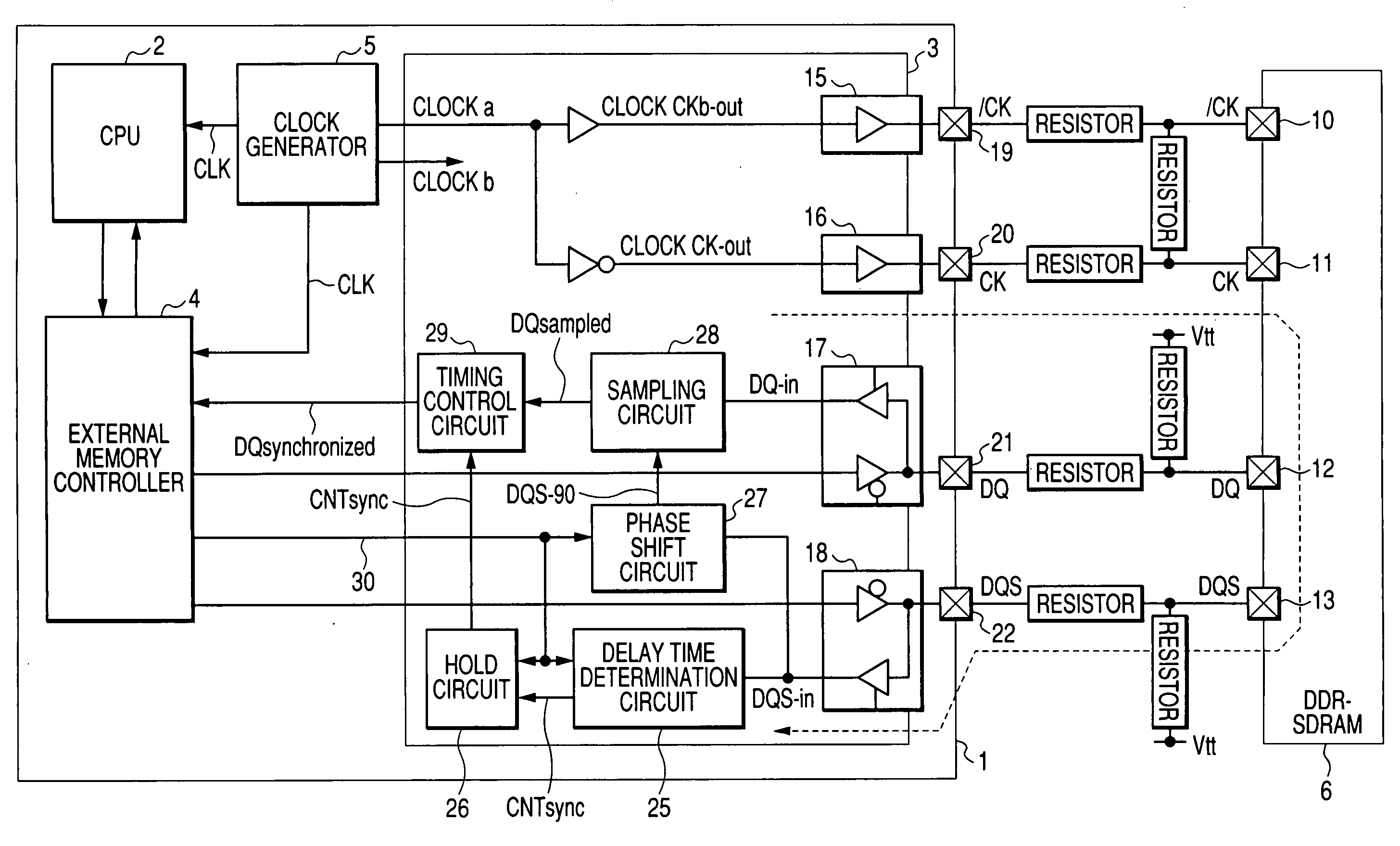
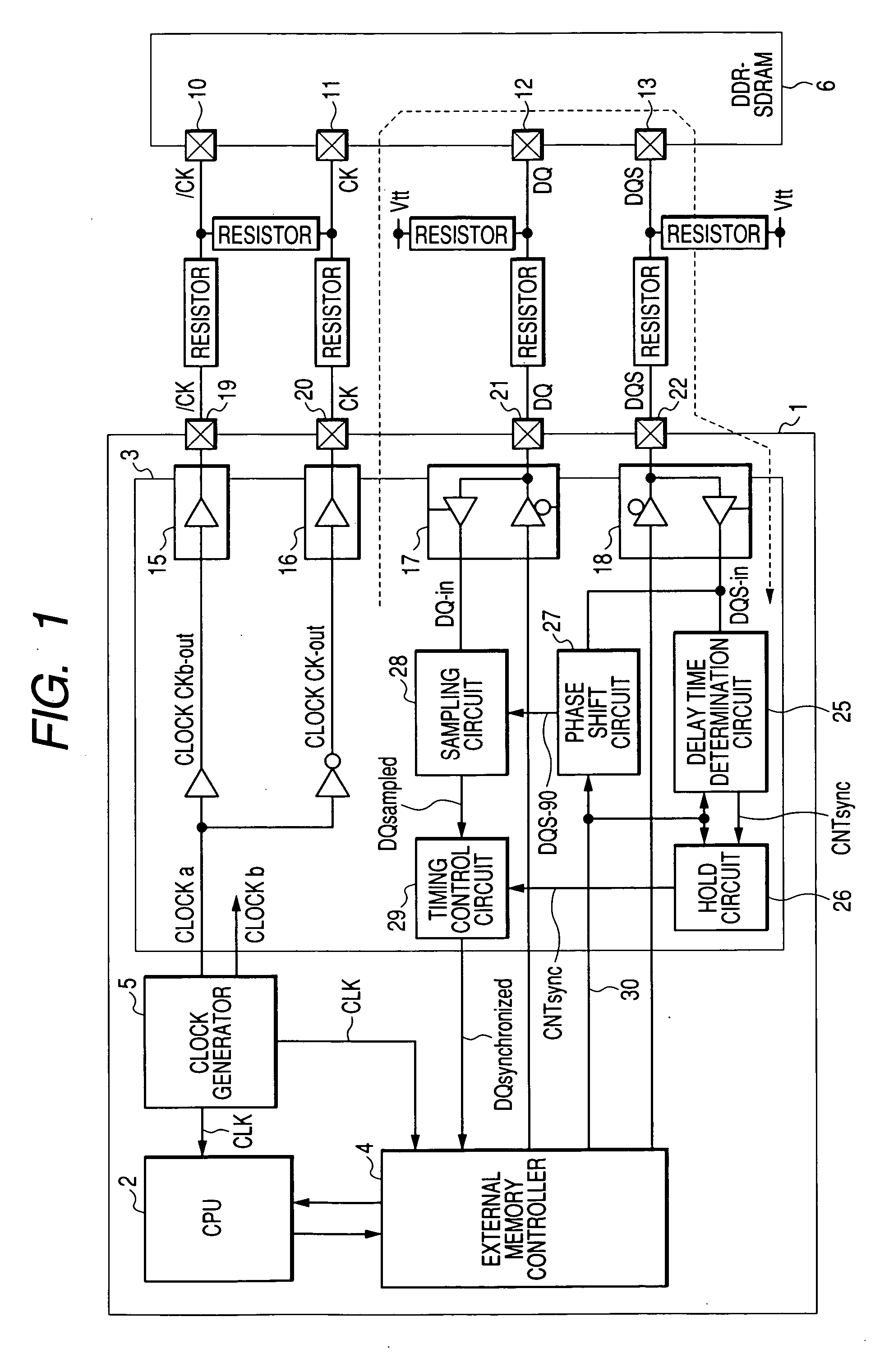
[0052] A data processor according to one embodiment of the present invention is shown in FIG. 1. Although not restricted in particular, the data processor 1 shown in the same figure is formed in one semiconductor substrate like monocrystal silicon by a complementary type MOS integrated circuit manufacturing technology or the like.

[0053] The data processor 1 includes a central processing unit (CPU) 2 used as a typically-shown data processing circuit, a memory interface circuit 3, an external memory controller 4 and a clock generator (clock generating circuit) 5. The CPU 2 has an instruction controller and an arithmetic unit. The instruction controller controls an instruction fetch and decodes a fetched instruction. The arithmetic unit performs a data operation or an address operation using the result of decoding of the instruction and an operand specified by the instruction to execute an instruction. The memory interface circuit 3 enables a DDR synchronous memory configured i...


PUM


Abstract

A memory interface circuit is connectable to a DDR-SDRAM which outputs read data in synchronization with a data strobe signal together with the data strobe signal. A clock generator generates internal clock signals and memory clock signals supplied to the DDR-SDRAM. The memory interface circuit determines a delay of arrival of the data strobe signal relative to the corresponding internal clock signal by using a data strobe signal inputted in a read cycle with respect to the DDR-SDRAM, samples the arrived read data, based on a signal obtained by shifting the phase of the arrived data strobe signal, and synchronizes the sampled read data to the corresponding internal clock signal on the basis of the result of determination of the arrival delay.

Description


Claims


Application Information

Patent Timeline
Owner RENESAS ELECTRONICS CORP
Why Eureka
Try Eureka